- 您現(xiàn)在的位置:買賣IC網 > PDF目錄8951 > SI5321-H-GL (Silicon Laboratories Inc)IC CLOCK MULT SONET/SDH 63LFBGA PDF資料下載
參數(shù)資料
| 型號: | SI5321-H-GL |
| 廠商: | Silicon Laboratories Inc |
| 文件頁數(shù): | 11/34頁 |
| 文件大小: | 0K |
| 描述: | IC CLOCK MULT SONET/SDH 63LFBGA |
| 標準包裝: | 260 |
| 系列: | DSPLL® |
| 類型: | 時鐘乘法器 |
| PLL: | 是 |
| 輸入: | LVTTL |
| 輸出: | CML |
| 電路數(shù): | 1 |
| 比率 - 輸入:輸出: | 1:1 |
| 差分 - 輸入:輸出: | 是/是 |
| 頻率 - 最大: | 2.8GHz |
| 除法器/乘法器: | 是/是 |
| 電源電壓: | 3.135 V ~ 3.465 V |
| 工作溫度: | -20°C ~ 85°C |
| 安裝類型: | 表面貼裝 |
| 封裝/外殼: | 63-LBGA |
| 供應商設備封裝: | 63-PBGA(9x9) |
| 包裝: | 托盤 |
第1頁第2頁第3頁第4頁第5頁第6頁第7頁第8頁第9頁第10頁當前第11頁第12頁第13頁第14頁第15頁第16頁第17頁第18頁第19頁第20頁第21頁第22頁第23頁第24頁第25頁第26頁第27頁第28頁第29頁第30頁第31頁第32頁第33頁第34頁
Si5321
Rev. 2.5
19
and setting FEC[2:0] = 001 (255/238 FEC scaling).
Finally, a 622.08 MHz output clock (a non-FEC rate) can
be generated from a 20.83 MHz input clock (an FEC
rate) by setting INFRQSEL[2:0] = 001 (19.44 MHz
range), setting FRQSEL[2:0] = 011 (32x multiplication)
and setting FEC[2:0] = 010 (238/255 FEC scaling).
2.3. PLL Performance
The Si5321 PLL provides extremely low jitter
generation, high jitter tolerance, and a well-controlled
jitter transfer function with low peaking and a high
degree of jitter attenuation.
2.3.1. Jitter Generation
Jitter generation is defined as the amount of jitter
produced at the output of the device with a jitter free
input clock. Generated jitter arises from sources within
the VCO and other PLL components. Jitter generation is
a function of the PLL bandwidth setting. Higher loop
bandwidth settings may result in lower jitter generation
but may also result in less attenuation of jitter than
might be present on the input clock signal.
2.3.2. Jitter Transfer
Jitter transfer is defined as the ratio of output signal jitter
to input signal jitter for a specified jitter frequency. The
jitter transfer characteristic determines the amount of
input clock jitter that passes to the outputs. The DSPLL
technology used in the Si5321 provides tightly-
controlled jitter transfer curves because the PLL gain
parameters are determined by digital circuits that do not
vary over supply voltage, process, and temperature. In
a system application, a well-controlled transfer curve
minimizes the output clock jitter variation from board to
board and provides more consistent system level jitter
performance.
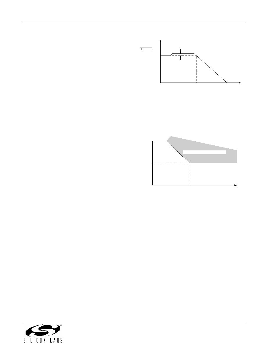
The jitter transfer characteristic is a function of the
BWSEL[1:0] setting. Lower bandwidth settings result in
more jitter attenuation of the incoming clock but may
result in higher jitter generation. Table 4 on page 10
gives the 3 dB bandwidth and peaking values for
specified BWSEL settings. Figure 6 shows the jitter
transfer curve mask.
.
Figure 6. PLL Jitter Transfer Mask/Template
2.3.3. Jitter Tolerance
Jitter tolerance for the Si5321 is defined as the
maximum peak-to-peak sinusoidal jitter that can be
present on the incoming clock. The tolerance is a
function of the jitter frequency because tolerance
improves for lower input jitter frequency.
Figure 7. Jitter Tolerance Mask/Template
2.4. Loss-of-Signal Alarm
The Si5321 has loss-of-signal (LOS) circuitry that
constantly monitors the CLKIN input clock for missing
pulses. The LOS circuitry sets a LOS output alarm
signal when missing pulses are detected.
The LOS circuitry operates as follows. Regardless of
the selected input clock frequency range, the LOS
circuitry divides down the input clock into the 19 MHz
range. The LOS circuitry then over-samples this divided
down input clock to search for extended periods of time
without input clock transitions. If the LOS circuitry
detects four consecutive samples of the divided down
input clock that are the same state (i.e., 1111 or 0000), a
LOS condition is declared; the Si5321 goes into digital
hold mode, and the LOS output alarm signal is set high.
The LOS sampling circuitry runs at a frequency of fO_78,
where fO_78 is the output clock frequency when the
FRQSEL[2:0] pins are set to 100. Figure 3 on page 5
and Table 3 on page 7 list the minimum and maximum
transitionless time periods required for declaring a LOS
on the input clock (tLOS).
Jitter
Transfer
0 dB
F
BW
f
Jitter
Peaking
–20 dB/dec.
Jitter Out
Jitter In
(s)
J
p
Input
Jitter
Amplitude
10 ns
F
BW
–20 dB/dec.
f
Jitter In
Excessive Input Jitter Range
相關PDF資料 |
PDF描述 |
|---|---|
| VE-JVJ-MZ-F3 | CONVERTER MOD DC/DC 36V 25W |
| VE-26H-MW-F2 | CONVERTER MOD DC/DC 52V 100W |
| VE-26H-MW-F1 | CONVERTER MOD DC/DC 52V 100W |
| VE-JVJ-MZ-F1 | CONVERTER MOD DC/DC 36V 25W |
| VE-JVP-MZ-F2 | CONVERTER MOD DC/DC 13.8V 25W |
相關代理商/技術參數(shù) |
參數(shù)描述 |
|---|---|
| SI5321-H-ZL2 | 制造商:Silicon Laboratories Inc 功能描述: |
| Si5321-XLNX-DC | 功能描述:子卡和OEM板 Silabs/Xilinx Ref Design RoHS:否 制造商:BeagleBoard by CircuitCo 產品:BeagleBone LCD4 Boards 用于:BeagleBone - BB-Bone - Open Source Development Kit |
| SI5322 | 制造商:SILABS 制造商全稱:SILABS 功能描述:Pin-Controlled 1_710 MHz Jitter Cleaning Clock |
| Si5322/23-EVB | 功能描述:時鐘和定時器開發(fā)工具 Si5322/Si5323 EVAL BOARD RoHS:否 制造商:Texas Instruments 產品:Evaluation Modules 類型:Clock Conditioners 工具用于評估:LMK04100B 頻率:122.8 MHz 工作電源電壓:3.3 V |
| Si5322-B-GM | 功能描述:時鐘合成器/抖動清除器 PIN-PROGRAMMABLE CLK MULTIPLIER 1 OUT RoHS:否 制造商:Skyworks Solutions, Inc. 輸出端數(shù)量: 輸出電平: 最大輸出頻率: 輸入電平: 最大輸入頻率:6.1 GHz 電源電壓-最大:3.3 V 電源電壓-最小:2.7 V 封裝 / 箱體:TSSOP-28 封裝:Reel |
發(fā)布緊急采購,3分鐘左右您將得到回復。