- 您現(xiàn)在的位置:買賣IC網(wǎng) > PDF目錄25644 > SI5338N-A00000-GMR (SILICON LABORATORIES) 700 MHz, PROC SPECIFIC CLOCK GENERATOR, QCC24 PDF資料下載
參數(shù)資料
| 型號: | SI5338N-A00000-GMR |
| 廠商: | SILICON LABORATORIES |
| 元件分類: | 時鐘產(chǎn)生/分配 |
| 英文描述: | 700 MHz, PROC SPECIFIC CLOCK GENERATOR, QCC24 |
| 封裝: | 4 X 4 MM, ROHS COMPLIANT, MO-220VGGD-8, QFN-24 |
| 文件頁數(shù): | 9/34頁 |
| 文件大?。?/td> | 285K |
| 代理商: | SI5338N-A00000-GMR |
第1頁第2頁第3頁第4頁第5頁第6頁第7頁第8頁當(dāng)前第9頁第10頁第11頁第12頁第13頁第14頁第15頁第16頁第17頁第18頁第19頁第20頁第21頁第22頁第23頁第24頁第25頁第26頁第27頁第28頁第29頁第30頁第31頁第32頁第33頁第34頁

Si5338
Rev. 0.5
17
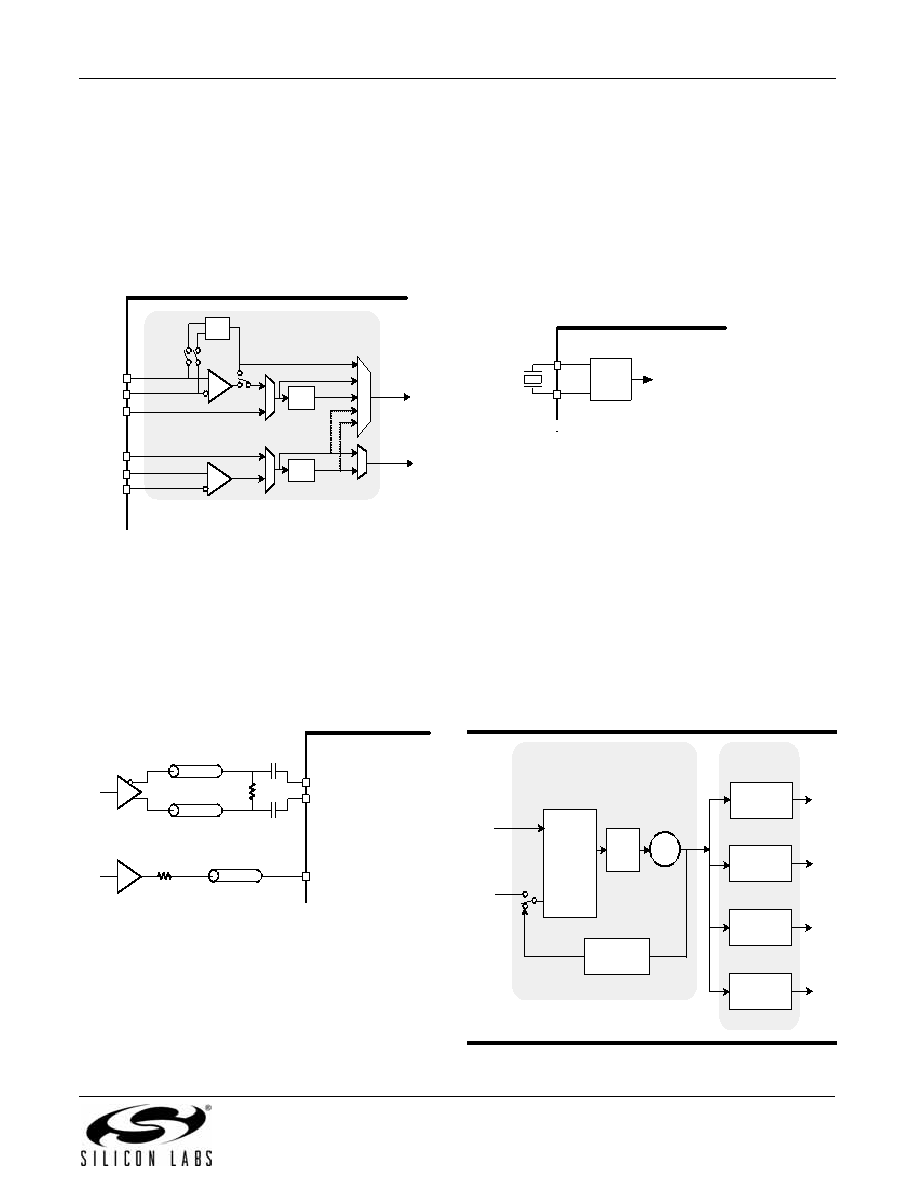
3.2. Input Stage
The input stage supports four inputs. Two are used as
the clock inputs to the synthesis stage and the other two
are used as feedback inputs for zero delay or external
feedback mode. In cases where external feedback is
not required, all four input are available to the synthesis
stage. The reference selector selects one of the inputs
as the reference to the synthesis stage. The input
configuration is selectable through the IC interface.
Figure 2. Input Stage
IN1/IN2 and IN5/IN6 are differential inputs which are
capable of accepting clock rates ranging from 5 MHz to
710 MHz.
The
differential
inputs
are
capable
of
interfacing to multiple signals such as LVPECL, LVDS,
HSCL, and CML. Differential signals must be AC
coupled as shown in Figure 3. A termination resistor of
100 Ohms placed close to the input pins is also
required. Refer to Table 6 for signal voltage limits.
Figure 3. Interfacing Differential and Single-
Ended Signals to the Si5338
IN3 and IN4 accept single-ended signals from 5 MHz to
200 MHz (CMOS) or 350 MHz (SSTL, HSTL). The
single-ended inputs are internally AC coupled so they
can accept a wide variety of signals without requiring a
specific DC level. The input signal only needs to meet a
minimum voltage swing which makes it compatible with
common single-ended signals such as CMOS, HSTL,
and SSTL. Refer to Table 6 for signal voltage limits. A
typical single-ended connection is shown in Figure 3.
Refer
to
application
note
AN408
for
additional
termination options.
For free-run operation, the internal oscillator can
operate from a low frequency fundamental mode crystal
(XTAL) with a resonant frequency between 8 and
30 MHz. A crystal can easily be connected to pins IN1
and IN2 without external components as shown in
Figure 4. Connecting an XTAL to the Si5338
Refer to application note AN360 for recommended
XTAL components.
3.3. Synthesis Stages
Synthesis of the output clocks is performed in two
stages as shown in Figure 5. The first stage is a high
frequency analog phase-locked loop (APLL) which
multiplies the input stage clock to a frequency within the
range of 2.2 GHz to 2.8 GHz. Multiplication of the input
frequency is accomplished using a proprietary and
highly precise MultiSynth feedback divider (N) which
allows the APLL to generate any frequency within its
VCO range with less jitter than typical fractional N
dividers.
Figure 5. Synthesis Stages
÷P2
÷P1
Osc
Input
Stage
fb
CLKIN
CLKINB
IN3
IN2
IN1
Clock
Inputs
Feedback
Inputs
IN6
IN4
IN5
FDBK
FDBKB
ref
Reference
Selector
To
Synthesis
Sta
g
e
osc
ref
refdiv
fb
fbdiv
IN2 / IN6
IN1 / IN5
100
50
0.1 uF
IN3 / IN4
50
Rs
IN2
IN1
XTAL
Osc
To synthesis stage
or output selectors
Phase
Frequency
Detector
Loop
Filter
VCO
MultiSynth
÷M0
MultiSynth
÷M1
MultiSynth
÷M2
MultiSynth
÷M3
MultiSynth
÷N
Synthesis
Stage 1
(APLL)
Synthesis
Stage 2
ref
fb
F
rom
Input
Stag
e
T
o
Output
S
tage
2.2-2.8
GHz
相關(guān)PDF資料 |
PDF描述 |
|---|---|
| SI5338N-AXXXXXGM | 700 MHz, PROC SPECIFIC CLOCK GENERATOR, QCC24 |
| SL28540ALCT | OTHER CLOCK GENERATOR, QCC56 |
| SL5504 | 1 CHANNEL TRANSISTOR OUTPUT OPTOCOUPLER |
| SL5582.3S | 1 CHANNEL TRANSISTOR OUTPUT OPTOCOUPLER |
| SLA-360MTT32S | T-1 SINGLE COLOR LED, YELLOW GREEN, 3.1 mm |
相關(guān)代理商/技術(shù)參數(shù) |
參數(shù)描述 |
|---|---|
| SI5338N-A00211-GMR | 制造商:Silicon Laboratories Inc 功能描述:CLOCK - Tape and Reel |
| SI5338N-A01659-GM | 制造商:Silicon Laboratories Inc 功能描述:CLOCK - Bulk |
| SI5338N-A01659-GMR | 制造商:Silicon Laboratories Inc 功能描述:CLOCK - Tape and Reel |
| Si5338N-A-GM | 功能描述:時鐘發(fā)生器及支持產(chǎn)品 I2C-prgrmmbl clock generatr .16-700 MHz RoHS:否 制造商:Silicon Labs 類型:Clock Generators 最大輸入頻率:14.318 MHz 最大輸出頻率:166 MHz 輸出端數(shù)量:16 占空比 - 最大:55 % 工作電源電壓:3.3 V 工作電源電流:1 mA 最大工作溫度:+ 85 C 安裝風(fēng)格:SMD/SMT 封裝 / 箱體:QFN-56 |
| SI5338N-A-GMR | 功能描述:時鐘發(fā)生器及支持產(chǎn)品 I2C Program Clk Gen 0.16-710MHz 4Clk In RoHS:否 制造商:Silicon Labs 類型:Clock Generators 最大輸入頻率:14.318 MHz 最大輸出頻率:166 MHz 輸出端數(shù)量:16 占空比 - 最大:55 % 工作電源電壓:3.3 V 工作電源電流:1 mA 最大工作溫度:+ 85 C 安裝風(fēng)格:SMD/SMT 封裝 / 箱體:QFN-56 |
發(fā)布緊急采購,3分鐘左右您將得到回復(fù)。