- 您現(xiàn)在的位置:買賣IC網(wǎng) > PDF目錄383838 > ST20GP6 MAX 7000 CPLD 256 MC 208-RQFP PDF資料下載
參數(shù)資料
| 型號: | ST20GP6 |
| 英文描述: | MAX 7000 CPLD 256 MC 208-RQFP |
| 中文描述: | GPS處理器 |
| 文件頁數(shù): | 52/116頁 |
| 文件大小: | 1107K |
| 代理商: | ST20GP6 |
第1頁第2頁第3頁第4頁第5頁第6頁第7頁第8頁第9頁第10頁第11頁第12頁第13頁第14頁第15頁第16頁第17頁第18頁第19頁第20頁第21頁第22頁第23頁第24頁第25頁第26頁第27頁第28頁第29頁第30頁第31頁第32頁第33頁第34頁第35頁第36頁第37頁第38頁第39頁第40頁第41頁第42頁第43頁第44頁第45頁第46頁第47頁第48頁第49頁第50頁第51頁當(dāng)前第52頁第53頁第54頁第55頁第56頁第57頁第58頁第59頁第60頁第61頁第62頁第63頁第64頁第65頁第66頁第67頁第68頁第69頁第70頁第71頁第72頁第73頁第74頁第75頁第76頁第77頁第78頁第79頁第80頁第81頁第82頁第83頁第84頁第85頁第86頁第87頁第88頁第89頁第90頁第91頁第92頁第93頁第94頁第95頁第96頁第97頁第98頁第99頁第100頁第101頁第102頁第103頁第104頁第105頁第106頁第107頁第108頁第109頁第110頁第111頁第112頁第113頁第114頁第115頁第116頁
ST20-GP1
52/116
the initial bus width of all banks after reset.
9.2
Strobe allocation
9.3
External accesses
The EMI differentiates accesses and transactions. An access is the lowest denominator of a
transaction. Since the ST20 word size is 32 bits, several accesses are required to complete a
transaction in most cases. The following are cases where several accesses may not be required:
CPU executes a sb(store byte), lb(load byte) or ss(store sixteen), ls(load sixteen) instruc-
tion.
CPU is executing a move2dnonzero(2D block copy non-zero bytes) or move2dzero(2D
block copy zero bytes) instruction and the data dictates that certain bytes are not to be
written.
The first or last DMA operation to or from a link is to a non word aligned byte address.
Figure 9.2 shows the generic EMI activity during a read access and the configurable parameters.
The rising edge of
notMemOE
always occurs at the end of the read access just after the data is
latched on chip.
notMemWB0
is always inactive during a read access.
notMemWB1
activity
during a read access depends on the bus width for the bank. The strobe is inactive if the bus width
is configured to be 16-bit. If the bus width is configured to be 8-bit,
notMemWB1
behaves as
address bit 0 with the same timing as
MemAddr1-19
.
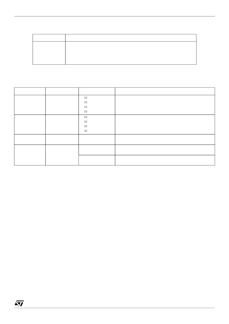
BootSource[1:0] Bootstrap start-up conditions
00
01
10
11
Boot from link. 16-bit bus width for all banks.
Boot from ROM. 8-bit bus width for all banks. Link operational.
Boot from ROM. 16-bit bus width for all banks. Link powered down.
Boot from ROM. 8-bit bus width for all banks. Link powered down.
Table 9.1
BootSource0-1
encoding
Pin
Bank allocation
Correspondence
Active access type
notMemCE0-3
1 per bank
0
bank 0
1
bank 1
2
bank 2
3
bank 3
0
bank 0
1
bank 1
2
bank 2
3
bank 3
MemData0-7
Reads and writes
notMemOE0-3
1 per bank
Reads only
notMemWB0
Shared amongst
all banks.
Shared amongst
all banks.
Writes only. Indicates valid write data on
MemData0-7
.
notMemWB1
16-bit bus:
MemData8-15
8-bit bus:
not applicable
Table 9.2 Strobe allocation
Writes only. Indicates valid write data on
MemData8-15
.
Reads and writes. Behaves as address bit 0 with same
timing as
MemAddr1-19
.
相關(guān)PDF資料 |
PDF描述 |
|---|---|
| ST25C02AB1 | IC FLEX 6000 FPGA 16K 144-TQFP |
| ST25C02AB6 | Stratix FPGA 25K FBGA-672 |
| ST25C02AM1 | IC ACEX 1K FPGA 100K 208-PQFP |
| ST25C02AM6 | Cyclone II FPGA 20K FBGA-256 |
| ST25C04ML1 | IC FLEX 6000 FPGA 24K 144-TQFP |
相關(guān)代理商/技術(shù)參數(shù) |
參數(shù)描述 |
|---|---|
| ST20-GP6 | 制造商:STMICROELECTRONICS 制造商全稱:STMicroelectronics 功能描述:GPS PROCESSOR |
| ST20GP6CT33S | 制造商:STMICROELECTRONICS 制造商全稱:STMicroelectronics 功能描述:GPS PROCESSOR |
| ST20GP6CX33S | 功能描述:射頻無線雜項(xiàng) GPS Processor RoHS:否 制造商:Texas Instruments 工作頻率:112 kHz to 205 kHz 電源電壓-最大:3.6 V 電源電壓-最小:3 V 電源電流:8 mA 最大功率耗散: 工作溫度范圍:- 40 C to + 110 C 封裝 / 箱體:VQFN-48 封裝:Reel |
| ST20GP6CX33STR | 功能描述:射頻無線雜項(xiàng) GPS Processor RoHS:否 制造商:Texas Instruments 工作頻率:112 kHz to 205 kHz 電源電壓-最大:3.6 V 電源電壓-最小:3 V 電源電流:8 mA 最大功率耗散: 工作溫度范圍:- 40 C to + 110 C 封裝 / 箱體:VQFN-48 封裝:Reel |
| ST20GP6X33S | 制造商:STMICROELECTRONICS 制造商全稱:STMicroelectronics 功能描述:GPS PROCESSOR |
發(fā)布緊急采購,3分鐘左右您將得到回復(fù)。