- 您現(xiàn)在的位置:買(mǎi)賣(mài)IC網(wǎng) > PDF目錄371182 > TDA8540T (NXP SEMICONDUCTORS) 4 X 4 video switch matrix PDF資料下載
參數(shù)資料
| 型號(hào): | TDA8540T |
| 廠(chǎng)商: | NXP SEMICONDUCTORS |
| 元件分類(lèi): | 運(yùn)動(dòng)控制電子 |
| 英文描述: | 4 X 4 video switch matrix |
| 中文描述: | 4-CHANNEL, AUDIO/VIDEO SWITCH, PDSO20 |
| 文件頁(yè)數(shù): | 5/20頁(yè) |
| 文件大小: | 131K |
| 代理商: | TDA8540T |
第1頁(yè)第2頁(yè)第3頁(yè)第4頁(yè)當(dāng)前第5頁(yè)第6頁(yè)第7頁(yè)第8頁(yè)第9頁(yè)第10頁(yè)第11頁(yè)第12頁(yè)第13頁(yè)第14頁(yè)第15頁(yè)第16頁(yè)第17頁(yè)第18頁(yè)第19頁(yè)第20頁(yè)

1995 Feb 06
5
Philips Semiconductors
Product specification
4
×
4 video switch matrix
TDA8540
FUNCTIONAL DESCRIPTION
The TDA8540 is controlled via a bidirectional I
2
C-bus.
3 bits of the I
2
C address can be selected via the address
pin, thus providing a facility for parallel connection of
7 devices.
Control options via the I
2
C-bus:
The input signals can be clamped at their negative peak
(top sync).
The gain factor of the outputs can be selected between
1
×
or 2
×
.
Each of the four outputs can individually be connected
to one of the four inputs.
Each output can individually be set in a high impedance
state.
Two binary output data lines can be controlled for
switching accompanying sound signals.
The SDA and SCL pins (pins 19 and 18) can be connected
to the I
2
C-bus or to DC switching voltage sources. Address
inputs S0 to S2 (pins 11, 7 and 5) are used to select
sub-addresses or switching to the non-I
2
C mode. Inputs
S0 to S2 can be connected to the supply voltage (HIGH) or
the ground (LOW). In this way no peripheral components
are required for selection.
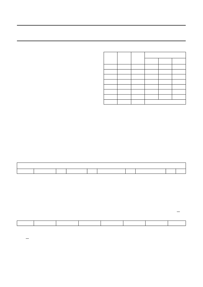
Table 1
I
2
C-bus sub-addressing
I
2
C-bus control
After power-up the outputs are initialized in the high
impedance state, and D0 and D1 are at a LOW level.
Detailed description of the I
2
C-bus specification, with
applications, is given in brochure “The I
2
C-bus and how to
use it” This brochure may be ordered using the code
9398 393 40011.
The TDA8540 is a
slave receiver
and the protocol is given
in Table 2.
S2
S1
S0
SUB-ADDRESS
A2
A1
A0
L
L
L
L
H
H
H
H
L
L
H
H
L
L
H
H
L
H
L
H
L
H
L
H
0
0
0
0
1
1
1
non I
2
C addressable
0
0
1
1
0
0
1
0
1
0
1
0
1
0
Table 2
The TDA8540 protocol
Notes
1.
2.
3.
4.
S = START condition.
Data transmission to the TDA8540 starts with the slave address (SLV).
A = acknowledge bit, generated by TDA8540.
P = STOP condition.
Table 3
Data transmission to the TDA8540 begins with SLV
Notes
1.
2.
A2 to A0: pin programmable slave address bits.
R/W = 0; write only.
After the SLV, a second byte, SUB, is required for selecting the functions, as shown in Table 4.
SEQUENCE
A
(3)
S
(1)
SLV
(2)
A
(3)
SUB
DATA
A
(3)
DATA
A
(3)
P
(4)
A6
MSB
A5
A4
A3
A2
A1
A0
R/W
LSB
0
(2)
1
0
0
1
A2
(1)
A1
(1)
A0
(1)
相關(guān)PDF資料 |
PDF描述 |
|---|---|
| TDA8540 | 4 X 4 video switch matrix |
| TDA8542AT | 2 x 1.5 W BTL audio amplifier |
| TDA8542 | 2 x 1 W BTL audio amplifier |
| TDA8542T | 2 x 1 W BTL audio amplifier |
| TDA8566 | 2 x 25 W BTL stereo car radio power amplifier with differential inputs and diagnostic outputs |
相關(guān)代理商/技術(shù)參數(shù) |
參數(shù)描述 |
|---|---|
| TDA8540TD-T | 制造商:未知廠(chǎng)家 制造商全稱(chēng):未知廠(chǎng)家 功能描述:Cross-Point Switch |
| TDA8541 | 制造商:PHILIPS 制造商全稱(chēng):NXP Semiconductors 功能描述:1 W BTL audio amplifier |
| TDA8541T | 制造商:NXP Semiconductors 功能描述:Audio Amplifier Circuit, Single, 8 Pin, Plastic, SOP |
| TDA8541T/N1 | 制造商:NXP Semiconductors 功能描述:Bulk 制造商:NXP Semiconductors 功能描述:AMP AUDIO PWR 1.2W MONO 8SOIC 制造商:NXP Semiconductors 功能描述:AMP, AUDIO, PWR, 1.2W, MONO, 8SOIC 制造商:NXP Semiconductors 功能描述:AMP, AUDIO, PWR, 1.2W, MONO, 8SOIC; Amplifier Class:AB; No. of Channels:1; Output Power:1.2W; Supply Voltage Range:2.2V to 18V; Amplifier Case Style:SOIC; No. of Pins:8; Load Impedance:8ohm; Operating Temperature Min:-40C; Operating;RoHS Compliant: Yes |
| TDA8541T/N1,112 | 功能描述:音頻放大器 AMP 7712 1W BTL RoHS:否 制造商:STMicroelectronics 產(chǎn)品:General Purpose Audio Amplifiers 輸出類(lèi)型:Digital 輸出功率: THD + 噪聲: 工作電源電壓:3.3 V 電源電流: 最大功率耗散: 最大工作溫度: 安裝風(fēng)格:SMD/SMT 封裝 / 箱體:TQFP-64 封裝:Reel |
發(fā)布緊急采購(gòu),3分鐘左右您將得到回復(fù)。