- 您現在的位置:買賣IC網 > PDF目錄373637 > TH50VSF2581AASB (Toshiba Corporation) Circular Connector; MIL SPEC:MIL-C-5015; Body Material:Metal; Series:GT; No. of Contacts:7; Connector Shell Size:18; Connecting Termination:Solder; Circular Shell Style:Square Flange Receptacle; Body Style:Straight PDF資料下載
參數資料
| 型號: | TH50VSF2581AASB |
| 廠商: | Toshiba Corporation |
| 元件分類: | 圓形連接器 |
| 英文描述: | Circular Connector; MIL SPEC:MIL-C-5015; Body Material:Metal; Series:GT; No. of Contacts:7; Connector Shell Size:18; Connecting Termination:Solder; Circular Shell Style:Square Flange Receptacle; Body Style:Straight |
| 中文描述: | SRAM和閃存混合多芯片封裝 |
| 文件頁數: | 19/50頁 |
| 文件大小: | 546K |
| 代理商: | TH50VSF2581AASB |
第1頁第2頁第3頁第4頁第5頁第6頁第7頁第8頁第9頁第10頁第11頁第12頁第13頁第14頁第15頁第16頁第17頁第18頁當前第19頁第20頁第21頁第22頁第23頁第24頁第25頁第26頁第27頁第28頁第29頁第30頁第31頁第32頁第33頁第34頁第35頁第36頁第37頁第38頁第39頁第40頁第41頁第42頁第43頁第44頁第45頁第46頁第47頁第48頁第49頁第50頁
TH50VSF2580/2581AASB
2001-10-26 19/50
SIMULTANEOUS READ/WRITE OPERATION
The TH50VSF2580/2581AASB features a Simultaneous Read/Write operation. The Simultaneous Read/Write
operation enables the device to simultaneously write data to or erase data from a bank while reading data from
another bank.
The TH50VSF2580/2581AASB has a total of nine banks: 1 bank of 0.5 Mbits, 1 bank of 3.5 Mbits and 7 banks of
4 Mbits. Banks can be switched between using the bank addresses (A20~A15). For a description of bank blocks and
addresses, please refer to the Block Address Table and Block Size Table.
The Simultaneous Read/Write operation cannot perform multiple operations within a single bank. The table
below shows the operation modes in which simultaneous operation can be performed.
Note that during Auto-Program execution or Auto Block Erase operation, the Simultaneous Read/Write operation
cannot read data from addresses in the same bank which have not been selected for operation. Data from these
addresses can be read using the Program Suspend or Erase Suspend function, however.
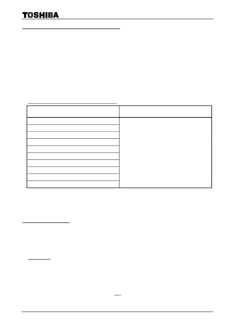
SIMULTANEOUS READ/WRITE OPERATION
STATUS OF
BANK ON WHICH OPERATION IS BEING
PERFORMED
STATUS OF OTHER BANKS
Read Mode
ID Read Mode
(1)
Auto-Program Mode
Fast Program Mode
(2)
Program Suspend Mode
Auto Block Erase Mode
Auto Multiple Block Erase Mode
(3)
Erase Suspend Mode
Program Suspend during Erase Suspend
CFI Mode
Read Mode
(1) Only Command Mode is valid.
(2) Including
times when Acceleration Mode is in use.
(3) If the selected blocks are spread across all nine banks, simultaneous operation cannot be carried out.
OPERATION MODES
In addition to the Read, Write and Erase Modes, the TH50VSF2520/2581AASB features many functions
including block protection and data polling. When incorporating the device into a deign, please refer to the timing
charts and flowcharts in combination with the description below.
Read Mode
To read data from the memory cell array, set the device to Read Mode. In Read Mode the device can perform
high-speed random access as asynchronous ROM.
The device is automatically set to Read Mode immediately after power-on or on completion of automatic
operation. A software reset releases ID Read Mode and the lock state which the device enters if automatic
operation ends abnormally, and sets the device to Read Mode. A hardware reset terminates operation of the
device and resets it to Read Mode. When reading data without changing the address immediately after
power-on, either input a hardware Reset or change CEF from H to L.
相關PDF資料 |
PDF描述 |
|---|---|
| TH50VSF3582AASB | TOSHIBA MULTI-CHIP INTEGRATED CIRCUIT SILICON GATE CMOS |
| TH50VSF3583AASB | TOSHIBA MULTI-CHIP INTEGRATED CIRCUIT SILICON GATE CMOS |
| TH50VSF3680 | 0.4W, 75V, 0.3A, SIGNAL DIODE, SOD123 |
| TH50VSF3681AASB | GT 10C 10#16 SKT RECP BOX RM |
| TH513 | RF & MICROWAVE TRANSISTORS HF SSB APPLICATIONS |
相關代理商/技術參數 |
參數描述 |
|---|---|
| TH50VSF2582 | 制造商:TOSHIBA 制造商全稱:Toshiba Semiconductor 功能描述:SRAM AND FLASH MEMORY MIXED MULTI-CHIP PACKAGE |
| TH50VSF2582AASB | 制造商:TOSHIBA 制造商全稱:Toshiba Semiconductor 功能描述:SRAM AND FLASH MEMORY MIXED MULTI-CHIP PACKAGE |
| TH50VSF2583AASB | 制造商:TOSHIBA 制造商全稱:Toshiba Semiconductor 功能描述:SRAM AND FLASH MEMORY MIXED MULTI-CHIP PACKAGE |
| TH50VSF3582AASB | 制造商:TOSHIBA 制造商全稱:Toshiba Semiconductor 功能描述:TOSHIBA MULTI-CHIP INTEGRATED CIRCUIT SILICON GATE CMOS |
| TH50VSF3583AASB | 制造商:TOSHIBA 制造商全稱:Toshiba Semiconductor 功能描述:TOSHIBA MULTI-CHIP INTEGRATED CIRCUIT SILICON GATE CMOS |
發(fā)布緊急采購,3分鐘左右您將得到回復。