- 您現(xiàn)在的位置:買(mǎi)賣(mài)IC網(wǎng) > PDF目錄98229 > THS770012IRGET (TEXAS INSTRUMENTS INC) SPECIALTY ANALOG CIRCUIT, PQCC24 PDF資料下載
參數(shù)資料
| 型號(hào): | THS770012IRGET |
| 廠(chǎng)商: | TEXAS INSTRUMENTS INC |
| 元件分類(lèi): | 模擬信號(hào)調(diào)理 |
| 英文描述: | SPECIALTY ANALOG CIRCUIT, PQCC24 |
| 封裝: | GREEN, PLASTIC, VQFN-24 |
| 文件頁(yè)數(shù): | 13/35頁(yè) |
| 文件大小: | 1305K |
| 代理商: | THS770012IRGET |
第1頁(yè)第2頁(yè)第3頁(yè)第4頁(yè)第5頁(yè)第6頁(yè)第7頁(yè)第8頁(yè)第9頁(yè)第10頁(yè)第11頁(yè)第12頁(yè)當(dāng)前第13頁(yè)第14頁(yè)第15頁(yè)第16頁(yè)第17頁(yè)第18頁(yè)第19頁(yè)第20頁(yè)第21頁(yè)第22頁(yè)第23頁(yè)第24頁(yè)第25頁(yè)第26頁(yè)第27頁(yè)第28頁(yè)第29頁(yè)第30頁(yè)第31頁(yè)第32頁(yè)第33頁(yè)第34頁(yè)第35頁(yè)

50W
200W
V
OCM
V
OUT-
200W
V
IN-
V
IN+
Filter
and
Bias
THS770012
V
OUT+
R
O
V
OCM
R
O
ADC
A
IN-
A
IN+
CM
SLOS669B
– FEBRUARY 2010 – REVISED MAY 2011
Operation with Split Supply
±2.5V
The THS770012 can be operated using a split
±2.5V supply. In this case, VS+ is connected to +2.5V, and GND
(and any other pin noted to be connected to GND) is connected to -2.5V. As with any device, the THS770012 is
impervious to what the user decides to name the levels in the system. In essence, it is simply a level shift of the
power pins by
–2.5V. If everything else is level-shifted by the same amount, the device sees no difference. With
a
±2.5V power supply, the VOCM range is 0V ±0.25V; therefore, power-down levels are –2.5V = on and +2.5V =
off, and input and output voltage ranges are symmetrical about 0V. This design has certain advantages in
systems where signals are referenced to ground, and as noted in the following section, for driving ADCs with low
input common-mode voltage requirements in dc-coupled applications.
Driving Capcitive Loads
The THS770012 is tested as described previously, with the data shown in the typical graphs. Due to the internal
gain resistor architecture used on the device, the only practical means to avoid stability problems such as
overshoot/ringing, gain peaking, and oscillation when driving capacitive loads is to place small resistors in series
with the outputs (RO) to isolate the phase shift caused by the capacitive load from the feedback loop of the
amplifier. Note there are 2
Ω internal resistors in series with each output to help maintain stability. The Typical
Characteristics graphs show recommended values for an optimally flat frequency response with maximum
bandwidth. Smaller values of RO can be used if more peaking is allowed, and larger values can be used to -
reduce the bandwidth.
Driving ADCs
The THS770012 is designed and optimized for the highest performance to drive differential input ADCs.
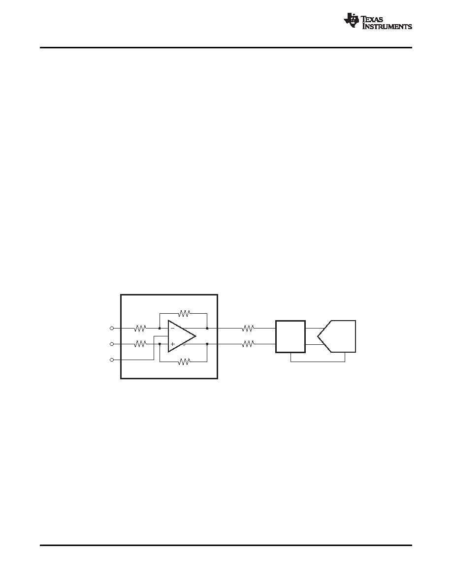
Figure 40 shows a generic block diagram of the THS770012 driving an ADC. The primary interface circuit
between the amplifier and the ADC is usually a filter of some type for antialias purposes, and provides a means
to bias the signal to the input common-mode voltage required by the ADC. Filters range from single-order real
RC poles to higher-order LC filters, depending on the requirements of the application. Output resistors (RO) are
shown on the amplifier outputs to isolate the amplifier from any capacitive loading presented by the filter.
Figure 40. Generic ADC Driver Block Diagram
The key points to consider for implementation are described in the following three subsections.
SNR Considerations
The signal-to-noise ratio (SNR) of the amplifier + filter + ADC adds in RMS fashion. Noise from the amplifier is
bandwidth-limited by the filter. Depending on the amplitude of the signal and the bandwidth of the filter, the SNR
of the amplifier + filter can be calculated. To get the combined SNR, this value is then squared, added to the
square of the ADC SNR, and the square-root is taken. If the SNR of the amplifier + filter equals the SNR of the
ADC, the combined SNR is 3dB higher and for minimal inpact on the ADC's SNR the SNR of the amplifier + filter
should be 10dB or more lower. The combined SNR calculated in this manner is usually accurate to within
±1dB
of actual implementation.
20
Copyright
2010–2011, Texas Instruments Incorporated
相關(guān)PDF資料 |
PDF描述 |
|---|---|
| THS8083-95CPZP | SPECIALTY CONSUMER CIRCUIT, PQFP100 |
| THS8083APZP | SPECIALTY CONSUMER CIRCUIT, PQFP100 |
| THS8083APZPG4 | SPECIALTY CONSUMER CIRCUIT, PQFP100 |
| THS8083CPZP | SPECIALTY CONSUMER CIRCUIT, PQFP100 |
| THS8133ACPHP | PARALLEL, WORD INPUT LOADING, 0.005 us SETTLING TIME, 10-BIT DAC, PQFP48 |
相關(guān)代理商/技術(shù)參數(shù) |
參數(shù)描述 |
|---|---|
| THS788 | 制造商:TI 制造商全稱(chēng):Texas Instruments 功能描述:QUAD-CHANNEL TIME MEASUREMENT UNIT (TMU) |
| THS788PFD | 功能描述:計(jì)時(shí)器和支持產(chǎn)品 Quad Ch Time Msmt Unit RoHS:否 制造商:Micrel 類(lèi)型:Standard 封裝 / 箱體:SOT-23 內(nèi)部定時(shí)器數(shù)量:1 電源電壓-最大:18 V 電源電壓-最小:2.7 V 最大功率耗散: 最大工作溫度:+ 85 C 最小工作溫度:- 40 C 封裝:Reel |
| THS788PFDT | 功能描述:計(jì)時(shí)器和支持產(chǎn)品 Quad Ch Time Msmt Unit RoHS:否 制造商:Micrel 類(lèi)型:Standard 封裝 / 箱體:SOT-23 內(nèi)部定時(shí)器數(shù)量:1 電源電壓-最大:18 V 電源電壓-最小:2.7 V 最大功率耗散: 最大工作溫度:+ 85 C 最小工作溫度:- 40 C 封裝:Reel |
| THS789PFD | 制造商:Texas Instruments 功能描述:Time Measurement Unit (TMU) 100-Pin HTQFP EP Tray 制造商:Texas Instruments 功能描述:IC TIME MEASUREMNT UNIT 100HTQFP 制造商:Texas Instruments 功能描述:THS789PFD |
| THS7BAT | 功能描述:電池組 Rechargeable NICD For THS700 series RoHS:否 制造商:Ultralife 電池大小: 電池?cái)?shù)量: 輸出電壓:3.7 V 容量: 化學(xué)性質(zhì):Lithium 端接類(lèi)型:Wire |
發(fā)布緊急采購(gòu),3分鐘左右您將得到回復(fù)。