- 您現(xiàn)在的位置:買賣IC網(wǎng) > PDF目錄368672 > TMS320C240PQL 16-Bit Microcontroller PDF資料下載
參數(shù)資料
| 型號(hào): | TMS320C240PQL |
| 英文描述: | 16-Bit Microcontroller |
| 中文描述: | 16位微控制器 |
| 文件頁(yè)數(shù): | 13/105頁(yè) |
| 文件大?。?/td> | 1481K |
| 代理商: | TMS320C240PQL |
第1頁(yè)第2頁(yè)第3頁(yè)第4頁(yè)第5頁(yè)第6頁(yè)第7頁(yè)第8頁(yè)第9頁(yè)第10頁(yè)第11頁(yè)第12頁(yè)當(dāng)前第13頁(yè)第14頁(yè)第15頁(yè)第16頁(yè)第17頁(yè)第18頁(yè)第19頁(yè)第20頁(yè)第21頁(yè)第22頁(yè)第23頁(yè)第24頁(yè)第25頁(yè)第26頁(yè)第27頁(yè)第28頁(yè)第29頁(yè)第30頁(yè)第31頁(yè)第32頁(yè)第33頁(yè)第34頁(yè)第35頁(yè)第36頁(yè)第37頁(yè)第38頁(yè)第39頁(yè)第40頁(yè)第41頁(yè)第42頁(yè)第43頁(yè)第44頁(yè)第45頁(yè)第46頁(yè)第47頁(yè)第48頁(yè)第49頁(yè)第50頁(yè)第51頁(yè)第52頁(yè)第53頁(yè)第54頁(yè)第55頁(yè)第56頁(yè)第57頁(yè)第58頁(yè)第59頁(yè)第60頁(yè)第61頁(yè)第62頁(yè)第63頁(yè)第64頁(yè)第65頁(yè)第66頁(yè)第67頁(yè)第68頁(yè)第69頁(yè)第70頁(yè)第71頁(yè)第72頁(yè)第73頁(yè)第74頁(yè)第75頁(yè)第76頁(yè)第77頁(yè)第78頁(yè)第79頁(yè)第80頁(yè)第81頁(yè)第82頁(yè)第83頁(yè)第84頁(yè)第85頁(yè)第86頁(yè)第87頁(yè)第88頁(yè)第89頁(yè)第90頁(yè)第91頁(yè)第92頁(yè)第93頁(yè)第94頁(yè)第95頁(yè)第96頁(yè)第97頁(yè)第98頁(yè)第99頁(yè)第100頁(yè)第101頁(yè)第102頁(yè)第103頁(yè)第104頁(yè)第105頁(yè)
TMS320C240, TMS320F240
DSP CONTROLLERS
SPRS042D – OCTOBER 1996 – REVISED NOVEMBER 1998
13
POST OFFICE BOX 1443
HOUSTON, TEXAS 77251–1443
description (continued)
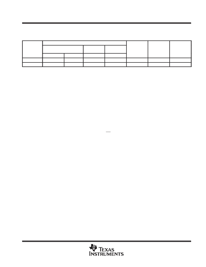
Table 1. Characteristics of the ’x240 DSP Controllers
ON-CHIP MEMORY (WORDS)
POWER
SUPPLY
(V)
CYCLE
TIME
(ns)
PACKAGE
TYPE
PIN COUNT
TMS320x240
DEVICES
RAM
ROM
FLASH
EEPROM
DATA
DATA/PROG
PROG
PROG
TMS320C240
288
256
16K
–
5
50
PQ 132–P
TMS320F240
288
256
–
16K
5
50
PQ 132–P
architectural overview
The functional block diagram provides a high-level description of each component in the ’x240 DSP controller.
The TMS320x240 devices are composed of three main functional units: a ’C2xx DSP core, internal memory,
and peripherals. In addition to these three functional units, there are several system-level features of the ’x240
that are distributed. These system features include the memory map, device reset, interrupts, digital
input/output (I/O), clock generation, and low-power operation.
system-level functions
device memory map
The TMS320x240 implements three separate address spaces for program memory, data memory, and I/O.
Each space accommodates a total of 64K 16-bit words. Within the 64K words of data space, the 256 to
32K words at the top of the address range can be defined to be external global memory in increments of powers
of two, as specified by the contents of the global memory allocation register (GREG). Access to global memory
is arbitrated using the global memory bus request (BR) signal.
On the ’x240, the first 96 (0–5Fh) data memory locations are either allocated for memory-mapped registers or
are reserved. This memory-mapped register space contains various control and status registers including those
for the CPU.
All the on-chip peripherals of the ’x240 device are mapped into data memory space. Access to these registers
is made by the CPU instructions addressing their data-memory locations. Figure 1 shows the memory map.
相關(guān)PDF資料 |
PDF描述 |
|---|---|
| TMS320C240PQQ | 16-Bit Microcontroller |
| TMS320F240PQL | 16-Bit Microcontroller |
| TMS320F240PQQ | 16-Bit Microcontroller |
| TMS320F240PQS | 16-Bit Microcontroller |
| TMS320LC31-40 | Digital Signal Processor |
相關(guān)代理商/技術(shù)參數(shù) |
參數(shù)描述 |
|---|---|
| TMS320C240PQQ | 制造商:未知廠家 制造商全稱:未知廠家 功能描述:16-Bit Microcontroller |
| TMS320C241 | 制造商:未知廠家 制造商全稱:未知廠家 功能描述:16-Bit Digital Signal Processor |
| TMS320C241FNS | 制造商:未知廠家 制造商全稱:未知廠家 功能描述:16-Bit Digital Signal Processor |
| TMS320C241PGS | 制造商:未知廠家 制造商全稱:未知廠家 功能描述:16-Bit Digital Signal Processor |
| TMS320C242 | 制造商:TI 制造商全稱:Texas Instruments 功能描述:DSP CONTROLLER |
發(fā)布緊急采購(gòu),3分鐘左右您將得到回復(fù)。