- 您現(xiàn)在的位置:買賣IC網(wǎng) > PDF目錄368672 > TMS320C240PQL 16-Bit Microcontroller PDF資料下載
參數(shù)資料
| 型號(hào): | TMS320C240PQL |
| 英文描述: | 16-Bit Microcontroller |
| 中文描述: | 16位微控制器 |
| 文件頁數(shù): | 85/105頁 |
| 文件大小: | 1481K |
| 代理商: | TMS320C240PQL |
第1頁第2頁第3頁第4頁第5頁第6頁第7頁第8頁第9頁第10頁第11頁第12頁第13頁第14頁第15頁第16頁第17頁第18頁第19頁第20頁第21頁第22頁第23頁第24頁第25頁第26頁第27頁第28頁第29頁第30頁第31頁第32頁第33頁第34頁第35頁第36頁第37頁第38頁第39頁第40頁第41頁第42頁第43頁第44頁第45頁第46頁第47頁第48頁第49頁第50頁第51頁第52頁第53頁第54頁第55頁第56頁第57頁第58頁第59頁第60頁第61頁第62頁第63頁第64頁第65頁第66頁第67頁第68頁第69頁第70頁第71頁第72頁第73頁第74頁第75頁第76頁第77頁第78頁第79頁第80頁第81頁第82頁第83頁第84頁當(dāng)前第85頁第86頁第87頁第88頁第89頁第90頁第91頁第92頁第93頁第94頁第95頁第96頁第97頁第98頁第99頁第100頁第101頁第102頁第103頁第104頁第105頁
T
D
S
P
8
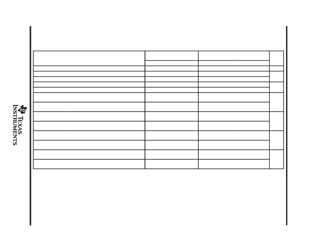
SPI MASTER MODE TIMING PARAMETERS
SPI master mode timing information is listed in the following tables.
SPI master mode external timing parameters (clock phase = 0)
(see Figure 43)
WHEN (SPIBRR + 1) IS EVEN OR
SPIBRR = 0 OR 2
WHEN (SPIBRR + 1)
IS ODD AND SPIBRR > 3
UNIT
MIN
4tc
MAX
128tc
0.5tc(SPC)M
0.5tc(SPC)M
0.5tc(SPC)M
0.5tc(SPC)M
MIN
5tc
MAX
127tc
tc(SPC)M
tw(SPCH)M§
tw(SPCL)M§
tw(SPCL)M§
tw(SPCH)M§
Cycle time, SPICLK
ns
Pulse duration, SPICLK high (clock polarity = 0)
0.5tc(SPC)M–70
0.5tc(SPC)M–70
0.5tc(SPC)M–70
0.5tc(SPC)M–70
0.5tc(SPC)M–0.5tc–70
0.5tc(SPC)M–0.5tc–70
0.5tc(SPC)M+0.5tc–70
0.5tc(SPC)M+0.5tc–70
0.5tc(SPC)M –0.5tc
0.5tc(SPC)M –0.5tc
0.5tc(SPC)M + 0.5tc
0.5tc(SPC)M + 0.5tc
ns
Pulse duration, SPICLK low (clock polarity = 1)
Pulse duration, SPICLK low (clock polarity = 0)
ns
Pulse duration, SPICLK high (clock polarity = 1)
td(SPCH-SIMO)M§
Delay time, SPICLK high (clock polarity = 0) to
SPISIMO valid
– 10
10
– 10
10
ns
td(SPCL-SIMO)M§
Delay time, SPICLK low (clock polarity = 1) to
SPISIMO valid
– 10
10
– 10
10
tv(SPCL-SIMO)M§
Valid time, SPISIMO data valid after SPICLK low
(clock polarity =0)
0.5tc(SPC)M–70
0.5tc(SPC)M+0.5tc–70
ns
tv(SPCH-SIMO)M§
Valid time, SPISIMO data valid after SPICLK high
(clock polarity =1)
0.5tc(SPC)M–70
0.5tc(SPC)M+0.5tc–70
tsu(SOMI-SPCL)M§
Setup time, SPISOMI before SPICLK low
(clock polarity = 0)
0
0
ns
tsu(SOMI-SPCH)M§
Setup time, SPISOMI before SPICLK high
(clock polarity = 1)
0
0
tv(SPCL-SOMI)M§
Valid time, SPISOMI data valid after SPICLK low
(clock polarity = 0)
0.25tc(SPC)M–70
0.5tc(SPC)M–0.5tc–70
ns
tv(SPCH-SOMI)M§
Valid time, SPISOMI data valid after SPICLK high
(clock polarity = 1)
0.25tc(SPC)M–70
0.5tc(SPC)M–0.5tc–70
The MASTER/SLAVE bit (SPICTL.2) is set and the CLOCK PHASE bit (SPICTL.3) is cleared.
tc = system clock cycle time = 1/SYSCLK = tc(SYS)
§The active edge of the SPICLK signal referenced is controlled by the CLOCK POLARITY bit (SPICCR.6).
相關(guān)PDF資料 |
PDF描述 |
|---|---|
| TMS320C240PQQ | 16-Bit Microcontroller |
| TMS320F240PQL | 16-Bit Microcontroller |
| TMS320F240PQQ | 16-Bit Microcontroller |
| TMS320F240PQS | 16-Bit Microcontroller |
| TMS320LC31-40 | Digital Signal Processor |
相關(guān)代理商/技術(shù)參數(shù) |
參數(shù)描述 |
|---|---|
| TMS320C240PQQ | 制造商:未知廠家 制造商全稱:未知廠家 功能描述:16-Bit Microcontroller |
| TMS320C241 | 制造商:未知廠家 制造商全稱:未知廠家 功能描述:16-Bit Digital Signal Processor |
| TMS320C241FNS | 制造商:未知廠家 制造商全稱:未知廠家 功能描述:16-Bit Digital Signal Processor |
| TMS320C241PGS | 制造商:未知廠家 制造商全稱:未知廠家 功能描述:16-Bit Digital Signal Processor |
| TMS320C242 | 制造商:TI 制造商全稱:Texas Instruments 功能描述:DSP CONTROLLER |
發(fā)布緊急采購,3分鐘左右您將得到回復(fù)。