- 您現在的位置:買賣IC網 > PDF目錄382684 > TQ5M34 Analog IC PDF資料下載
參數資料
| 型號: | TQ5M34 |
| 英文描述: | Analog IC |
| 中文描述: | 模擬IC |
| 文件頁數: | 11/18頁 |
| 文件大小: | 207K |
| 代理商: | TQ5M34 |

TQ5M34
Data Sheet
For additional information and latest specifications, see our website:
www.triquint.com
11
S-PARAMETERS:
We are often asked to provide S-parameters for our devices.
In the case of LNA’s the solution is straightforward. However,
for mxers such as the TQ5M31 and TQ5M34, the S-
parameters are totally dependant on the LO tuning inductor
(L2), the GIC pin bias components, and the mxer LO input
drive level. This is especially true for the RF input impedance.
Even the IF amplifier output (pin2) impedance is a weak
function of LO tuning. Thus the best we can do is to give S-
parameter plots of a typical board tuned to a particular band.
In all likelihood, The TQ5M34 in an application in the same
band with a different board layout, dielectric thickness, etc will
have different S-Parameters. They are likely, however, to at
least be in the same area of the Smth Chart.
Even changing the package of L2 will have an effect. For
example an 0603 sized inductor will have higher Q than an
0402, thus drive level will increase and the RF input
impedance will change. Thus there is no substitute for bench
experimentation and verification of tuning with this device.
SUGGESTED STEPS FOR TQ5M34 TUNING:
The following order of steps is recommended for applying the
TQ5M34. They are described in detail in the following
sections:
1. Lay out board consistent with the grounding guidelines at
the beginning of this note.
2. Experimentally determne proper LO tuning components.
This step needs to be done first since all of the later tuning is
affected by it.
3. Determne a tentative GIC network. It will have to be fine-
tuned later, since the image filter interaction will affect device
current.
4. Synthesize a tentative IF output match. It may have to be
fine-tuned later, as the final GIC configuration affects IF stage
current. LO is turned ON.
5. Experimentally determne a tentative RF Input match. LO
is turned ON.
6. Add the image filter to the circuit, and verify that the device
has adequate IP3. If not, another RF Input matching topology
can be tried.
7. Fine tune GIC components for needed Idd. LO is turned
ON.
8. Check IF match to see if it still is adequate. LO is turned
ON.
LO TUNING:
The drain of the LO buffer is brought out to pin 8 where it is
fed DC bias via an inductor. The inductor resonates with the
internal and external parasitic capacitance associated with
that pin. For maximumperformance the resonance must be
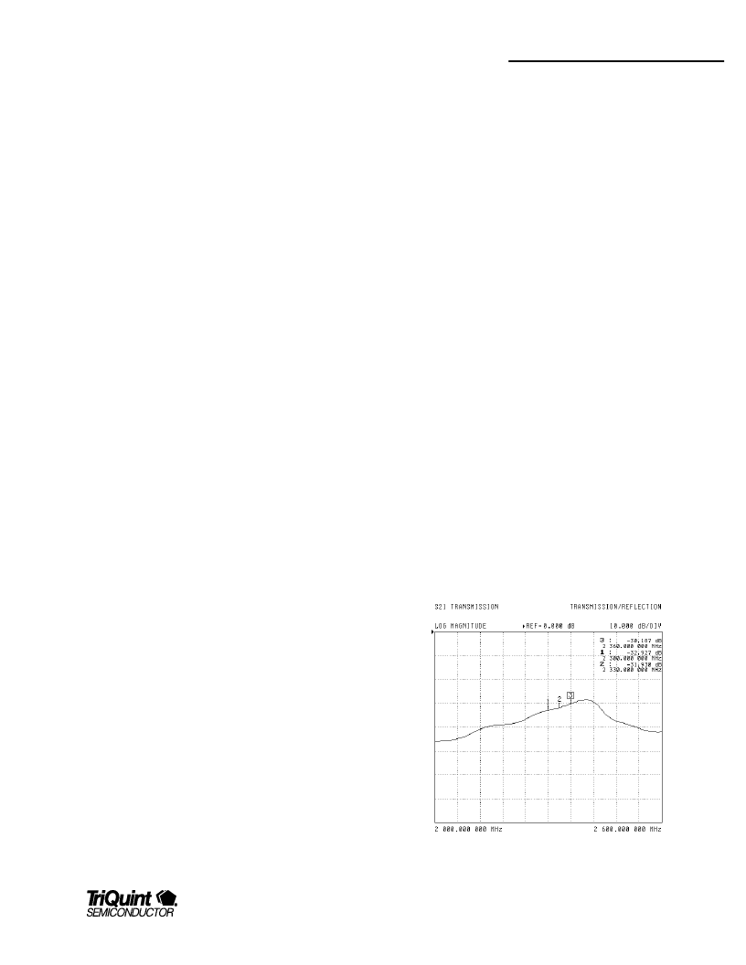
at or near the desired LO frequency. Figure 4 shows a
properly tuned LO buffer. Notice that the LO frequency range
of interest is to the left of the peak. We recommend that the
LO is tuned slightly higher in frequency, so that the desired
band is on the lower, more gradual side of the slope. Thus
there is less change in performance versus frequency. We
have also found empirically that tuning the LO slightly higher
in frequency results in much better LO input and RF input
matches.
Figure 4: Suggested LO Buffer Tuning
相關PDF資料 |
PDF描述 |
|---|---|
| TQ8214 | Industrial Control IC |
| TQ8219 | Optoelectronic |
| TQ8223 | ATM/SONET Demultiplexer |
| TQ8224 | Industrial Control IC |
| TQ8318 | Telecommunication IC |
相關代理商/技術參數 |
參數描述 |
|---|---|
| TQ5M44 | 制造商:TRIQUINT 制造商全稱:TriQuint Semiconductor 功能描述:RF Mixer IC |
| TQ6111BI | 制造商:未知廠家 制造商全稱:未知廠家 功能描述:Converter IC |
| TQ6111BV | 制造商:未知廠家 制造商全稱:未知廠家 功能描述:Converter IC |
| TQ6111D | 制造商:未知廠家 制造商全稱:未知廠家 功能描述:Converter IC |
| TQ6111M | 制造商:未知廠家 制造商全稱:未知廠家 功能描述:Converter IC |
發(fā)布緊急采購,3分鐘左右您將得到回復。