- 您現(xiàn)在的位置:買賣IC網(wǎng) > PDF目錄384045 > UPD72852GB-8EU (NEC Corp.) MOS INTEGRATED CIRCUIT PDF資料下載
參數(shù)資料
| 型號(hào): | UPD72852GB-8EU |
| 廠商: | NEC Corp. |
| 英文描述: | MOS INTEGRATED CIRCUIT |
| 中文描述: | 馬鞍山集成電路 |
| 文件頁數(shù): | 7/48頁 |
| 文件大小: | 249K |
| 代理商: | UPD72852GB-8EU |
第1頁第2頁第3頁第4頁第5頁第6頁當(dāng)前第7頁第8頁第9頁第10頁第11頁第12頁第13頁第14頁第15頁第16頁第17頁第18頁第19頁第20頁第21頁第22頁第23頁第24頁第25頁第26頁第27頁第28頁第29頁第30頁第31頁第32頁第33頁第34頁第35頁第36頁第37頁第38頁第39頁第40頁第41頁第42頁第43頁第44頁第45頁第46頁第47頁第48頁
Data Sheet S14920EJ3V0DS
7
μ
PD72852
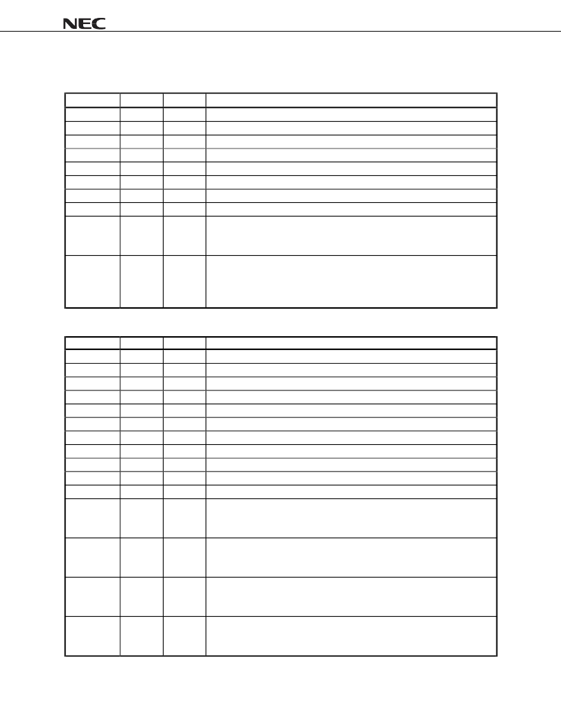
1. PIN FUNCTIONS
1.1 Cable Interface Pins
Name
Pin No.
I/O
Function
TpA0p
39
I/O
Port 0 twisted pair cable A positive phase I/O
TpA0n
38
I/O
Port 0 twisted pair cable A negative phase I/O
TpB0p
37
I/O
Port 0 twisted pair cable B positive phase I/O
TpB0n
36
I/O
Port 0 twisted pair cable B negative phase I/O
TpA1p
46
I/O
Port 1 twisted pair cable A positive phase I/O
TpA1n
45
I/O
Port 1 twisted pair cable A negative phase I/O
TpB1p
44
I/O
Port 1 twisted pair cable B positive phase I/O
TpB1n
43
I/O
Port 1 twisted pair cable B negative phase I/O
SUS/RES
19
I
Suspend/Resume function select
1: Suspend/Resume on (IEEE1394a-2000 compliant)
0: Suspend/Resume off (P1394a draft 1.3 compliant)
CPS
32
I
Cable power status
Connect to the cable through a 390 k
resistor and to GND through a 100 k
resistor.
0: Cable power fail
1: Cable power on
1.2 Link Interface Pins
Name
Pin No.
I/O
Function
D0
8
I/O
Data input/output (bit 0)
D1
9
I/O
Data input/output (bit 1)
D2
11
I/O
Data input/output (bit 2)
D3
12
I/O
Data input/output (bit 3)
D4
14
I/O
Data input/output (bit 4)
D5
15
I/O
Data input/output (bit 5)
D6
17
I/O
Data input/output (bit 6)
D7
18
I/O
Data input/output (bit 7)
CTL0
5
I/O
Link interface control (bit 0)
CTL1
6
I/O
Link interface control (bit 1)
LREQ
63
I
Link request input
SCLK
2
O
Link control output clock
LPS 1: 49.152 MHz output
LPS 0: Clamp to 0 (The clock signal will be output within 25
μ
sec after change to “0”)
LPS
59
I
Link power status input
0: Link power off
1: Link power on (PHY/Link direct connection)
LKON
58
O
Link-on signal output
Link-on signal is 6.144 MHz clock output.
Please refer to
4.2 Link-on Indication
.
DIRECT
50
I
PHY/Link isolation barrier control input
0: Isolation barrier
1: PHY/Link direct connection
相關(guān)PDF資料 |
PDF描述 |
|---|---|
| UPD72870F1 | IEEE1394 1-CHIP OHCI HOST CONTROLLER |
| UPD72870FA2 | IEEE1394 1-CHIP OHCI HOST CONTROLLER |
| UPD72871F1 | IEEE1394 1-CHIP OHCI HOST CONTROLLER |
| UPD72871FA2 | IEEE1394 1-CHIP OHCI HOST CONTROLLER |
| UPD72873 | MOS INTEGRATED CIRCUIT |
相關(guān)代理商/技術(shù)參數(shù) |
參數(shù)描述 |
|---|---|
| UPD74HC04C | 制造商:Panasonic Industrial Company 功能描述:IC |
| UPD750068GT-396 | 制造商:Renesas Electronics Corporation 功能描述: |
| UPD7507C189 | 制造商:Panasonic Industrial Company 功能描述:IC |
| UPD7508CU265 | 制造商:Panasonic Industrial Company 功能描述:IC |
| UPD75208 | 制造商:Panasonic Industrial Company 功能描述:IC |
發(fā)布緊急采購,3分鐘左右您將得到回復(fù)。