- 您現(xiàn)在的位置:買賣IC網(wǎng) > PDF目錄384045 > UPD72870F1 (NEC Corp.) IEEE1394 1-CHIP OHCI HOST CONTROLLER PDF資料下載
參數(shù)資料
| 型號(hào): | UPD72870F1 |
| 廠商: | NEC Corp. |
| 英文描述: | IEEE1394 1-CHIP OHCI HOST CONTROLLER |
| 中文描述: | IEEE1394連接1 - OHCI主機(jī)控制器芯片 |
| 文件頁(yè)數(shù): | 15/48頁(yè) |
| 文件大小: | 311K |
| 代理商: | UPD72870F1 |
第1頁(yè)第2頁(yè)第3頁(yè)第4頁(yè)第5頁(yè)第6頁(yè)第7頁(yè)第8頁(yè)第9頁(yè)第10頁(yè)第11頁(yè)第12頁(yè)第13頁(yè)第14頁(yè)當(dāng)前第15頁(yè)第16頁(yè)第17頁(yè)第18頁(yè)第19頁(yè)第20頁(yè)第21頁(yè)第22頁(yè)第23頁(yè)第24頁(yè)第25頁(yè)第26頁(yè)第27頁(yè)第28頁(yè)第29頁(yè)第30頁(yè)第31頁(yè)第32頁(yè)第33頁(yè)第34頁(yè)第35頁(yè)第36頁(yè)第37頁(yè)第38頁(yè)第39頁(yè)第40頁(yè)第41頁(yè)第42頁(yè)第43頁(yè)第44頁(yè)第45頁(yè)第46頁(yè)第47頁(yè)第48頁(yè)
Preliminary Data Sheet S13925EJ2V0DS00
15
μ
PD72870,72871
(2/2)
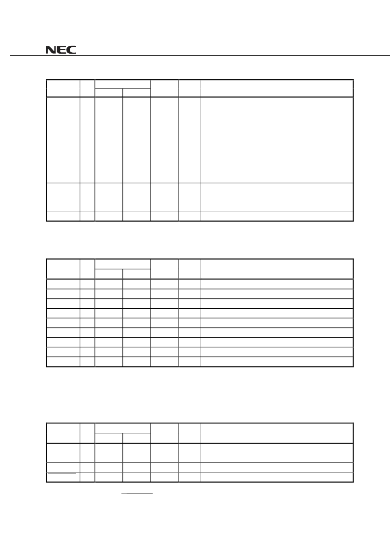
Pin No.
Name
I/O
LQFP
FPBGA
I
OL
Volts(V)
Function
PORTDIS
I
105
H16
Port Disable
SUS_RESM = “1”
This selected state will be loaded to Disabled bit which
allocated PHY register Port Status Page.
1:Disable
At this time, all ports will be disabled (
μ
PD72870: 3ports,
μ
PD72871: 1port).
SUS_RESM=“0”
PORTDIS has no effect.
SUS_RESM
I
106
G15
Suspend/Resume Function Select
1 : Suspend/Resume On (P1394a draft 2.0 compliant)
0 : Suspend/Resume Off (P1394a draft 1.3 compliant)
CPS
I
123
A15
-
-
Cable Power Status Input
Note
Note
Please refer to
4.1.3 CPS
.
1.3 PHY Signals: (9 pins)
Pin No.
Name
I/O
LQFP
FPBGA
I
OL
Volts(V)
Function
TpBias0
O
128
C14
-
-
Port-1 Twisted Pair Bias Voltage Output
Note 2
TpBias1
Note1
O
127
B14
-
-
Port-2 Twisted Pair Bias Voltage Output
Note 2
TpBias2
Note1
O
126
A14
-
-
Port-3 Twisted Pair Bias Voltage Output
Note 2
RI0
-
121
A16
-
-
Resistor0 for Reference Current Setting
Note 3
RI1
-
122
B16
-
-
Resistor1 for Reference Current Setting
Note 3
FIL1
-
114
E15
-
-
APLL Filter Terminal
(No need to assemble)
FIL0
-
115
E16
-
-
APLL Filter GND
(No need to assemble)
XI
I
117
D15
-
-
X’tal XI
XO
O
118
D16
-
-
X’tal XO
Note 1.
μ
PD72870 only. In
μ
PD72871, it is open.
2.
If unused port, please refer to
4.1.4 Unused Port
.
3.
Please refer to
4.5 RI0, RI1
.
1.4 PHY Control Signals: (5 pins)
Pin No.
Name
I/O
LQFP
FPBGA
I
OL
Volts(V)
Function
PC0-PC2
I
93-95
K15,L15,
L16
-
3.3
Power Class Input
Note 1
CMC
I
96
K16
-
3.3
Configuration Manager Capable
Note 1
P_RESETB
I
110
F16
PHY Power on Reset Input
Note 2
Note 1.
Please refer to
4.3 PC0-PC2, CMC
.
2.
Please refer to
4.4 P_RESETB
.
#
#
相關(guān)PDF資料 |
PDF描述 |
|---|---|
| UPD72870FA2 | IEEE1394 1-CHIP OHCI HOST CONTROLLER |
| UPD72871F1 | IEEE1394 1-CHIP OHCI HOST CONTROLLER |
| UPD72871FA2 | IEEE1394 1-CHIP OHCI HOST CONTROLLER |
| UPD72873 | MOS INTEGRATED CIRCUIT |
| UPD72873GC-YEB | MOS INTEGRATED CIRCUIT |
相關(guān)代理商/技術(shù)參數(shù) |
參數(shù)描述 |
|---|---|
| UPD74HC04C | 制造商:Panasonic Industrial Company 功能描述:IC |
| UPD750068GT-396 | 制造商:Renesas Electronics Corporation 功能描述: |
| UPD7507C189 | 制造商:Panasonic Industrial Company 功能描述:IC |
| UPD7508CU265 | 制造商:Panasonic Industrial Company 功能描述:IC |
| UPD75208 | 制造商:Panasonic Industrial Company 功能描述:IC |
發(fā)布緊急采購(gòu),3分鐘左右您將得到回復(fù)。