- 您現在的位置:買賣IC網 > PDF目錄383983 > UPD75236GJ (NEC Corp.) DIODE ZENER SINGLE 500mW 75Vz 1.7mA-Izt 0.05 0.1uA-Ir 56Vr DO35-GLASS 5K/AMMO PDF資料下載
參數資料
| 型號: | UPD75236GJ |
| 廠商: | NEC Corp. |
| 英文描述: | DIODE ZENER SINGLE 500mW 75Vz 1.7mA-Izt 0.05 0.1uA-Ir 56Vr DO35-GLASS 5K/AMMO |
| 中文描述: | 4位單片機 |
| 文件頁數: | 107/190頁 |
| 文件大小: | 1220K |
| 代理商: | UPD75236GJ |
第1頁第2頁第3頁第4頁第5頁第6頁第7頁第8頁第9頁第10頁第11頁第12頁第13頁第14頁第15頁第16頁第17頁第18頁第19頁第20頁第21頁第22頁第23頁第24頁第25頁第26頁第27頁第28頁第29頁第30頁第31頁第32頁第33頁第34頁第35頁第36頁第37頁第38頁第39頁第40頁第41頁第42頁第43頁第44頁第45頁第46頁第47頁第48頁第49頁第50頁第51頁第52頁第53頁第54頁第55頁第56頁第57頁第58頁第59頁第60頁第61頁第62頁第63頁第64頁第65頁第66頁第67頁第68頁第69頁第70頁第71頁第72頁第73頁第74頁第75頁第76頁第77頁第78頁第79頁第80頁第81頁第82頁第83頁第84頁第85頁第86頁第87頁第88頁第89頁第90頁第91頁第92頁第93頁第94頁第95頁第96頁第97頁第98頁第99頁第100頁第101頁第102頁第103頁第104頁第105頁第106頁當前第107頁第108頁第109頁第110頁第111頁第112頁第113頁第114頁第115頁第116頁第117頁第118頁第119頁第120頁第121頁第122頁第123頁第124頁第125頁第126頁第127頁第128頁第129頁第130頁第131頁第132頁第133頁第134頁第135頁第136頁第137頁第138頁第139頁第140頁第141頁第142頁第143頁第144頁第145頁第146頁第147頁第148頁第149頁第150頁第151頁第152頁第153頁第154頁第155頁第156頁第157頁第158頁第159頁第160頁第161頁第162頁第163頁第164頁第165頁第166頁第167頁第168頁第169頁第170頁第171頁第172頁第173頁第174頁第175頁第176頁第177頁第178頁第179頁第180頁第181頁第182頁第183頁第184頁第185頁第186頁第187頁第188頁第189頁第190頁
107
μ
PD75236
(7)
SCK0 pin output manipulation
Because the SCK0/P01 pin incorporates an output latch, static output is possible by software in addition
to normal serial clocks.
P01 output latch manipulation enables to set any number of SCK0 by software (SO0/SB0/SI0/SB1 pin is
controlled by the RELT and CMDT bits of SBIC).
SCK0/P01 pin output manipulation is described below.
Set the serial operating mode register 0 (CSIM0) (SCK0 pin: output mode, serial operation: enabled).
While serial transfer is stopped, SCK0 from the serial clock control circuit remains 1.
Manipulate the P01 output latch by a bit manipulation instruction.
Example
1 clock output to SCK0/P01 pin by software.
SEL
MB15
MOV
XA,#10000011B
MOV
CSIM0,XA
CLR1
0FF0H.1
SET1
0FF0H.1
; or CLR1 MBE
; SCK0(f
X
/2
3
), output mode
; SCK0/P01
←
0
; SCK0/P01
←
1
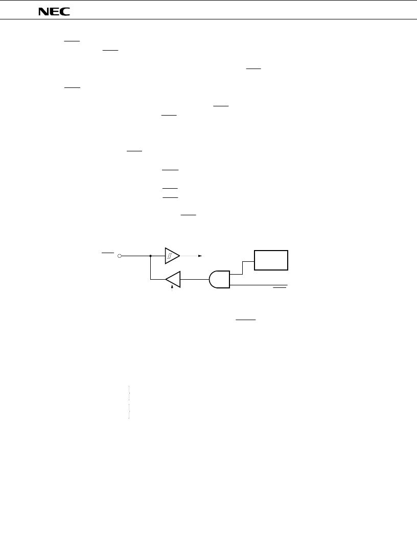
Fig. 4-58 SCK0/P01 Pin Configuration
The P01 output latch is mapped at bit 1 of address FF0H. RESET signal generation sets the P01 output
latch to “1”.
Note
1. It is necessary to set the P01 output latch to 1 during normal serial transfer.
2. The P01 output latch address cannot be set by “PORT0.1” as shown below. Describe address
(0FF0H.1) directly for the operand.
However, it is necessary to preset MBE = 0 or (MBE = 1 and MBS = 15) for instruction execution.
CLR1
PORT0.1
SET1
PORT0.1
CLR1
0FF0H.1
SET1
0FF0H.1
P01/SCK0
SCK0
P01 Output
Latch
and CSIM00
≠
00
Address
FF0H.1
To Internal
Circuit
From Serial Clock
Control Circuit
CSIEO = 1 and CSIM01
Use disabled
Use enabled
相關PDF資料 |
PDF描述 |
|---|---|
| UPD75236 | 4-BIT SINGLE-CHIP MICROCOMPUTER |
| UPD75516 | 4-BIT, SINGLE-CHIP CMOS MICROCOMPUTER WITH EXTENSIVE I/O AND A/D CONVERTER |
| UPD75516GF-637-3B9 | 4-BIT SINGLE-CHIP MICROCOMPUTER |
| UPD75516GF-076 | 4-BIT SINGLE-CHIP MICROCOMPUTER |
| UPD75516GF-079 | 4-BIT SINGLE-CHIP MICROCOMPUTER |
相關代理商/技術參數 |
參數描述 |
|---|---|
| UPD753012AGC-P33-8BT-A | 制造商:Renesas Electronics Corporation 功能描述: |
| UPD753016AGC-P29-8BT | 制造商:Renesas Electronics Corporation 功能描述: |
| UPD75304GF-407-3B9 | 制造商:Renesas Electronics Corporation 功能描述: |
| UPD75306G182 | 制造商:Panasonic Industrial Company 功能描述:IC |
| UPD75308F478 | 制造商:Panasonic Industrial Company 功能描述:IC |
發(fā)布緊急采購,3分鐘左右您將得到回復。