- 您現(xiàn)在的位置:買賣IC網(wǎng) > PDF目錄245649 > W3H32M64EA-533SBC (WHITE ELECTRONIC DESIGNS CORP) 32M X 64 DDR DRAM, PBGA208 PDF資料下載
參數(shù)資料
| 型號: | W3H32M64EA-533SBC |
| 廠商: | WHITE ELECTRONIC DESIGNS CORP |
| 元件分類: | DRAM |
| 英文描述: | 32M X 64 DDR DRAM, PBGA208 |
| 封裝: | 16 X 20 MM, 1 MM PITCH, PLASTIC, BGA-208 |
| 文件頁數(shù): | 27/28頁 |
| 文件大小: | 1057K |
| 代理商: | W3H32M64EA-533SBC |
第1頁第2頁第3頁第4頁第5頁第6頁第7頁第8頁第9頁第10頁第11頁第12頁第13頁第14頁第15頁第16頁第17頁第18頁第19頁第20頁第21頁第22頁第23頁第24頁第25頁第26頁當前第27頁第28頁
8
White Electronic Designs Corporation (602) 437-1520 www.whiteedc.com
White Electronic Designs
February 2010 2010 White Electronic Designs Corp. All rights reserved
Rev. 0
ADVANCED
White Electronic Designs Corp. reserves the right to change products or specications without notice.
W3H32M64EA-XSBX
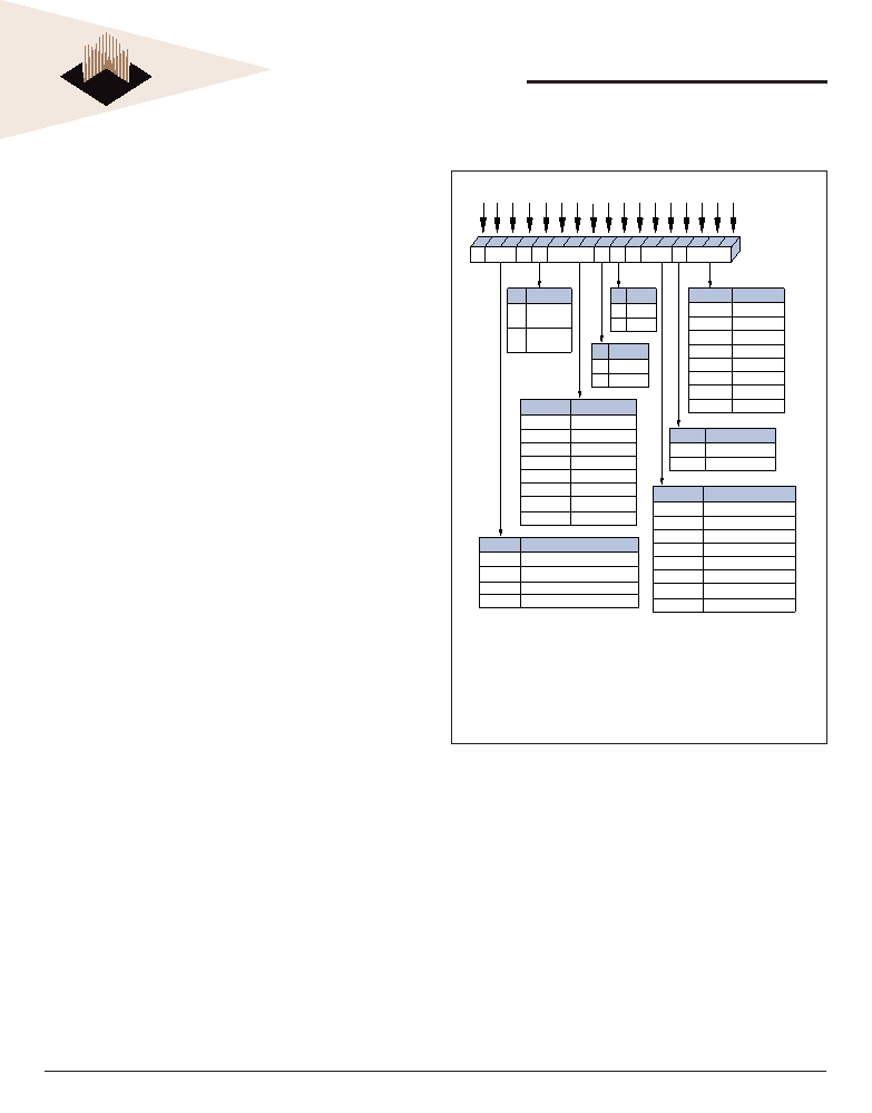
MODE REGISTER (MR)
The mode register is used to dene the specic mode of
operation of the DDR2 SDRAM. This denition includes
the selection of a burst length, burst type, CL, operating
mode, DLL RESET, write recovery, and power-down mode,
as shown in Figure 5. Contents of the mode register can be
altered by re-executing the LOAD MODE (LM) command.
If the user chooses to modify only a subset of the MR
variables, all variables (M0–M14) must be programmed
when the command is issued.
The mode register is programmed via the LM command
(bits BA1–BA0 = 0, 0) and other bits (M12–M0) will retain
the stored information until it is programmed again or
the device loses power (except for bit M8, which is self-
clearing). Reprogramming the mode register will not alter
the contents of the memory array, provided it is performed
correctly.
The LM command can only be issued (or reissued) when all
banks are in the precharged state (idle state) and no bursts
are in progress. The controller must wait the specied
time tMRD before initiating any subsequent operations
such as an ACTIVE command. Violating either of these
requirements will result in unspecied operation.
BURST LENGTH
Burst length is dened by bits M0–M3, as shown in Figure
5. Read and write accesses to the DDR2 SDRAM are
burst-oriented, with the burst length being programmable
to either four or eight. The burst length dete rmines
the maximum number of column locations that can be
accessed for a given READ or WRITE command.
When a READ or WRITE command is issued, a block of
columns equal to the burst length is effectively selected.
All accesses for that burst take place within this block,
meaning that the burst will wrap within the block if a
boundary is reached. The block is uniquely selected by
A2–Ai when BL = 4 and by A3–Ai when BL = 8 (where
Ai is the most signicant column address bit for a given
conguration). The remaining (least signicant) address
bit(s) is (are) used to select the starting location within the
block. The programmed burst length applies to both READ
and WRITE bursts.
BURST TYPE
Accesses within a given burst may be programmed to be
either sequential or interleaved. The burst type is selected
via bit M3, as shown in Figure 5. The ordering of accesses
within a burst is determined by the burst length, the burst
type, and the starting column address, as shown in Table
2. DDR2 SDRAM supports 4-bit burst mode and 8-bit burst
mode only. For 8-bit burst mode, full interleave address
ordering is supported; however, sequential address
ordering is nibble-based.
Burst Length
CAS#
BT
PD
A9
A7 A6 A5 A4 A3
A8
A2 A1 A0
Mode Register (Mx)
Address Bus
9
76543
8
210
A10
A12 A11
BA0
BA1
10
11
12
n
0
14
Burst Length
Reserved
4
8
Reserved
M0
0
1
0
1
0
1
0
1
M1
0
1
0
1
M2
0
1
0
1
Burst Type
Sequential
Interleaved
M3
CAS Latency (CL)
Reserved
3
4
5
6
7
M4
0
1
0
1
0
1
0
1
M5
0
1
0
1
M6
0
1
0
1
Mode
Normal
Test
M7
15
DLL TM
0
1
DLL Reset
No
Yes
M8
Write Recovery
Reserved
2
3
4
5
6
7
8
M9
0
1
0
1
0
1
0
1
M10
0
1
0
1
M11
0
1
WR
An
2
MR
M14
0
1
0
1
Mode Register Definition
Mode register (MR)
Extended mode register (EMR)
Extended mode register (EMR2)
Extended mode register (EMR3)
M15
0
1
M12
0
1
PD Mode
Fast exit
(normal)
Slow exit
(low power)
Latency
16
BA2
1
FIGURE 5 – MODE REGISTER (MR) DEFINITION
Notes:
1.
M16 (BA2) is only applicable for densities ≥1Gb, reserved for future use,
and must be programmed to “0.”
2.
Mode bits (Mn) with corresponding address balls (An) greater than M12
(A12) are reserved for future use and must be programmed to “0.”
3.
Not all listed WR and CL options are supported in any individual speed
grade.
相關PDF資料 |
PDF描述 |
|---|---|
| WF512K32F-70G2UC5A | 512K X 32 FLASH 5V PROM MODULE, 70 ns, CQMA68 |
| WE128K32-300HQ | 512K X 8 EEPROM 5V MODULE, 300 ns, CPGA66 |
| WE128K32-300G2C | 128K X 32 EEPROM 5V MODULE, 300 ns, CQFP68 |
| WF2M32I-90HM5 | 2M X 32 FLASH 5V PROM MODULE, 90 ns, CPGA66 |
| W7NCF512H11CSAHG | 32M X 16 FLASH 3.3V PROM CARD, 150 ns, UUC |
相關代理商/技術參數(shù) |
參數(shù)描述 |
|---|---|
| W3H32M64E-ES | 制造商:WEDC 制造商全稱:White Electronic Designs Corporation 功能描述:32M x 64 DDR2 SDRAM 208 PBGA Multi-Chip Package |
| W3H32M64E-ESC | 制造商:WEDC 制造商全稱:White Electronic Designs Corporation 功能描述:32M x 64 DDR2 SDRAM 208 PBGA Multi-Chip Package |
| W3H32M64E-ESI | 制造商:WEDC 制造商全稱:White Electronic Designs Corporation 功能描述:32M x 64 DDR2 SDRAM 208 PBGA Multi-Chip Package |
| W3H32M64E-ESM | 制造商:WEDC 制造商全稱:White Electronic Designs Corporation 功能描述:32M x 64 DDR2 SDRAM 208 PBGA Multi-Chip Package |
| W3H32M64E-SB | 制造商:WEDC 制造商全稱:White Electronic Designs Corporation 功能描述:32M x 64 DDR2 SDRAM 208 PBGA Multi-Chip Package |
發(fā)布緊急采購,3分鐘左右您將得到回復。