- 您現(xiàn)在的位置:買賣IC網(wǎng) > PDF目錄361786 > W530H Analog IC PDF資料下載
參數(shù)資料
| 型號: | W530H |
| 英文描述: | Analog IC |
| 中文描述: | 模擬IC |
| 文件頁數(shù): | 1/8頁 |
| 文件大小: | 184K |
| 代理商: | W530H |
Frequency Multiplying, Peak Reducing EMI Solution
W530
Cypress Semiconductor Corporation
3901 North First Street
San Jose
CA 95134
408-943-2600
November 22, 2000
Features
Cypress PREMIS family offering
Generates an EMI optimized clocking signal at the out-
put
Selectable output frequency range
Single 1.25%, 2.5%, 5% or 10% down or center spread
output
Integrated loop filter components
Operates with a 3.3 or 5V supply
Low power CMOS design
Available in 20-pin SSOP (Small Shrunk Outline
Package)
Key Specifications
Supply Voltages:.........................................V
DD
= 3.3V±0.3V
or V
DD
= 5V±10%
Frequency range: ............................13 MHz
≤
F
in
≤
120 MHz
Cycle to Cycle Jitter: .........................................250 ps (max)
Output duty cycle: .................................40/60% (worst case)
PREMIS is a trademark of Cypress Semiconductor.
W
20
19
18
17
16
1
2
3
4
5
6
7
8
9
10
X1
X2
AVDD
MW0^
STOP^
OR1^
NC
GND
REFOUT
VDD
GND
IR1*
IR2*
SSOUT
MW1*
GND
14
13
15
11
12
VDD
MW2^
OR2*
SSON#^
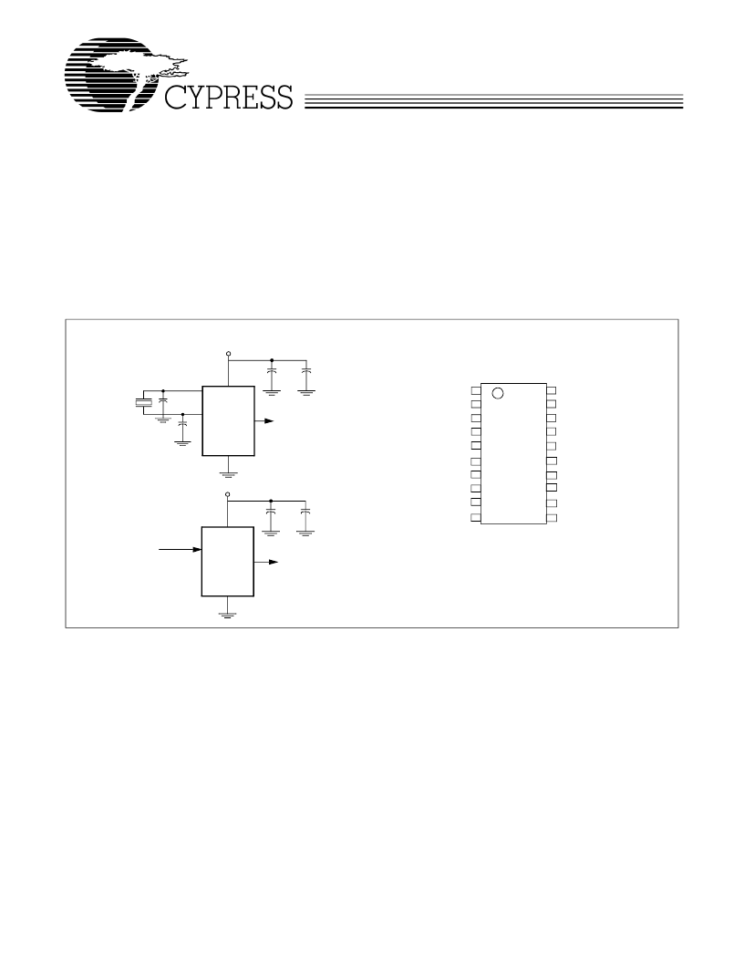
Simplified Block Diagram
Pin Configuration
SSOP
Spread Spectrum
Output
W530
(EMI suppressed)
3.3V or 5.0V
Oscillator or
Reference Input
Spread Spectrum
W530
(EMI suppressed)
3.3V or 5.0V
Input
X1
X2
X1
Note:
1.
Pins marked with ^ are internal pull-down resistors
with weak 250
.
Pins marked with * are internal
pull-up resistors with weak 250
.
[1]
相關(guān)PDF資料 |
PDF描述 |
|---|---|
| W532 | Clocks and Buffers |
| W532 | Frequency Multiplying, Peak Reducing EMI Solution(頻率倍增, 峰值減小EMI解決方案) |
| W53322 | |
| W53342 | |
| W5360120A | |
相關(guān)代理商/技術(shù)參數(shù) |
參數(shù)描述 |
|---|---|
| W5313 | 制造商:Tamura Corporation of America 功能描述: |
| W532 | 制造商:CYPRESS 制造商全稱:Cypress Semiconductor 功能描述:Frequency Multiplying, Peak Reducing EMI Solution |
| W5320-T0G | 制造商:Leviton Manufacturing Co 功能描述: |
| W5320-T0W | 制造商:Leviton Manufacturing Co 功能描述: |
| W532G | 制造商:Cypress Semiconductor 功能描述:CLOCK PARTS |
發(fā)布緊急采購,3分鐘左右您將得到回復(fù)。