- 您現(xiàn)在的位置:買賣IC網(wǎng) > PDF目錄245661 > W986432EH-7 (WINBOND ELECTRONICS CORP) 2M X 32 SYNCHRONOUS DRAM, 5.5 ns, PDSO86 PDF資料下載
參數(shù)資料
| 型號(hào): | W986432EH-7 |
| 廠商: | WINBOND ELECTRONICS CORP |
| 元件分類: | DRAM |
| 英文描述: | 2M X 32 SYNCHRONOUS DRAM, 5.5 ns, PDSO86 |
| 封裝: | 0.400 INCH, TSOP2-86 |
| 文件頁(yè)數(shù): | 48/48頁(yè) |
| 文件大小: | 1180K |
| 代理商: | W986432EH-7 |
第1頁(yè)第2頁(yè)第3頁(yè)第4頁(yè)第5頁(yè)第6頁(yè)第7頁(yè)第8頁(yè)第9頁(yè)第10頁(yè)第11頁(yè)第12頁(yè)第13頁(yè)第14頁(yè)第15頁(yè)第16頁(yè)第17頁(yè)第18頁(yè)第19頁(yè)第20頁(yè)第21頁(yè)第22頁(yè)第23頁(yè)第24頁(yè)第25頁(yè)第26頁(yè)第27頁(yè)第28頁(yè)第29頁(yè)第30頁(yè)第31頁(yè)第32頁(yè)第33頁(yè)第34頁(yè)第35頁(yè)第36頁(yè)第37頁(yè)第38頁(yè)第39頁(yè)第40頁(yè)第41頁(yè)第42頁(yè)第43頁(yè)第44頁(yè)第45頁(yè)第46頁(yè)第47頁(yè)當(dāng)前第48頁(yè)
W986432EH / W9864G2EH
Publication Release Date: August 17 ,2005
- 9 -
Revision A09
7.11 Burst Stop Command
A Burst Stop Command may be used to terminate the existing burst operation but leave the bank open
for future Read or Write Commands to the same page of the active bank, if the burst length is full
page. Use of the Burst Stop Command during other burst length operations is illegal. The Burst Stop
Command is defined by having RAS and CAS high with CS and WE low at the rising edge of
the clock. The data DQs go to a high impedance state after a delay, which is equal to the CAS
Latency in a burst read cycle, interrupted by Burst Stop. If a Burst Stop Command is issued during a
full page burst write operation, then any residual data from the burst write cycle will be ignored.
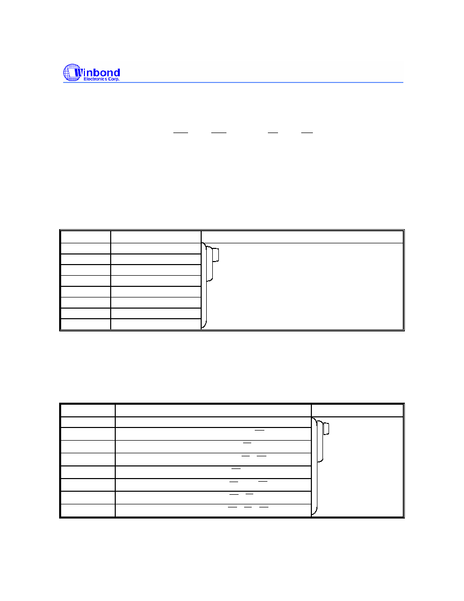
7.12 Addressing Sequence of Sequential Mode
A column access is performed by increasing the address from the column address which is input to
the device. The disturb address is varied by the Burst Length as shown in Table 2.
Table 2 Address Sequence of Sequential Mode
DATA
ACCESS ADDRESS
BURST LENGTH
Data 0
n
BL = 2 (disturb address is A0)
Data 1
n + 1
No address carry from A0 to A1
Data 2
n + 2
BL = 4 (disturb addresses are A0 and A1)
Data 3
n + 3
No address carry from A1 to A2
Data 4
n + 4
Data 5
n + 5
BL = 8 (disturb addresses are A0, A1 and A2)
Data 6
n + 6
No address carry from A2 to A3
Data 7
n + 7
7.13 Addressing Sequence of Interleave Mode
A column access is started in the input column address and is performed by inverting the address bit
in the sequence shown in Table 3.
Table 3 Address Sequence of Interleave Mode
DATA
ACCESS ADDRESS
BUST LENGTH
Data 0
A8 A7 A6 A5 A4 A3 A2 A1 A0
BL = 2
Data 1
A8 A7 A6 A5 A4 A3 A2 A1 A0
Data 2
A8 A7 A6 A5 A4 A3 A2 A1 A0
BL = 4
Data 3
A8 A7 A6 A5 A4 A3 A2 A1 A0
Data 4
A8 A7 A6 A5 A4 A3 A2 A1 A0
BL = 8
Data 5
A8 A7 A6 A5 A4 A3 A2 A1 A0
Data 6
A8 A7 A6 A5 A4 A3 A2 A1 A0
Data 7
A8 A7 A6 A5 A4 A3 A2 A1 A0
相關(guān)PDF資料 |
PDF描述 |
|---|---|
| W25X40-VSSI-G | 4M X 1 FLASH 2.7V PROM, PDSO8 |
| WF2M16W-90DAI5A | 2M X 16 FLASH 5V PROM MODULE, 90 ns, CDSO56 |
| WF2M16W-120DLM5A | 2M X 16 FLASH 5V PROM MODULE, 120 ns, CDSO44 |
| WF2M16W-90DAM5A | 2M X 16 FLASH 5V PROM MODULE, 90 ns, CDSO56 |
| WF2M16W-120DAC5A | 2M X 16 FLASH 5V PROM MODULE, 120 ns, CDSO56 |
相關(guān)代理商/技術(shù)參數(shù) |
參數(shù)描述 |
|---|---|
| W9864G2DH6 | 制造商:WINBOND 功能描述:New |
| W9864G2GH | 制造商:WINBOND 制造商全稱:Winbond 功能描述:512K X 4 BANKS X 32BITS SDRAM |
| W9864G2GH-5 | 制造商:WINBOND 制造商全稱:Winbond 功能描述:512K X 4 BANKS X 32BITS SDRAM |
| W9864G2GH-6 | 制造商:WINBOND 制造商全稱:Winbond 功能描述:512K X 4 BANKS X 32BITS SDRAM |
| W9864G2GH-6C | 制造商:WINBOND 制造商全稱:Winbond 功能描述:512K X 4 BANKS X 32BITS SDRAM |
發(fā)布緊急采購(gòu),3分鐘左右您將得到回復(fù)。