- 您現(xiàn)在的位置:買(mǎi)賣(mài)IC網(wǎng) > PDF目錄371341 > XC5210-6PQ240I Field Programmable Gate Array (FPGA) PDF資料下載
參數(shù)資料
| 型號(hào): | XC5210-6PQ240I |
| 英文描述: | Field Programmable Gate Array (FPGA) |
| 中文描述: | 現(xiàn)場(chǎng)可編程門(mén)陣列(FPGA) |
| 文件頁(yè)數(shù): | 38/73頁(yè) |
| 文件大小: | 598K |
| 代理商: | XC5210-6PQ240I |
第1頁(yè)第2頁(yè)第3頁(yè)第4頁(yè)第5頁(yè)第6頁(yè)第7頁(yè)第8頁(yè)第9頁(yè)第10頁(yè)第11頁(yè)第12頁(yè)第13頁(yè)第14頁(yè)第15頁(yè)第16頁(yè)第17頁(yè)第18頁(yè)第19頁(yè)第20頁(yè)第21頁(yè)第22頁(yè)第23頁(yè)第24頁(yè)第25頁(yè)第26頁(yè)第27頁(yè)第28頁(yè)第29頁(yè)第30頁(yè)第31頁(yè)第32頁(yè)第33頁(yè)第34頁(yè)第35頁(yè)第36頁(yè)第37頁(yè)當(dāng)前第38頁(yè)第39頁(yè)第40頁(yè)第41頁(yè)第42頁(yè)第43頁(yè)第44頁(yè)第45頁(yè)第46頁(yè)第47頁(yè)第48頁(yè)第49頁(yè)第50頁(yè)第51頁(yè)第52頁(yè)第53頁(yè)第54頁(yè)第55頁(yè)第56頁(yè)第57頁(yè)第58頁(yè)第59頁(yè)第60頁(yè)第61頁(yè)第62頁(yè)第63頁(yè)第64頁(yè)第65頁(yè)第66頁(yè)第67頁(yè)第68頁(yè)第69頁(yè)第70頁(yè)第71頁(yè)第72頁(yè)第73頁(yè)

R
XC5200 Series Field Programmable Gate Arrays
7-120
November 5, 1998 (Version 5.2)
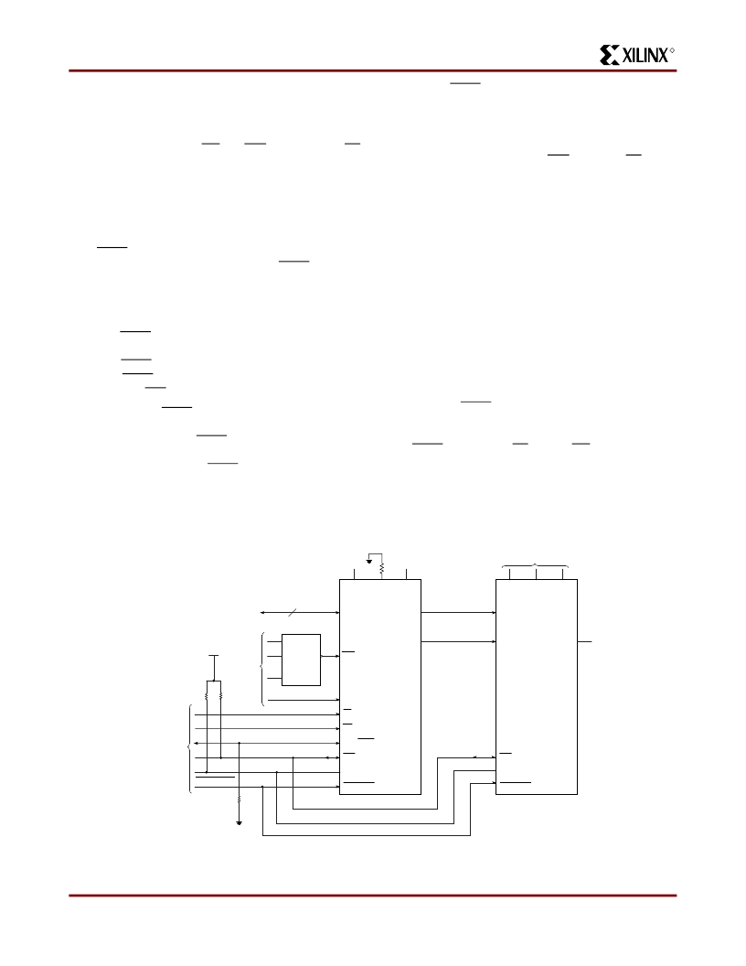
Asynchronous Peripheral Mode
Write to FPGA
Asynchronous Peripheral mode uses the trailing edge of
the logic AND condition of WS and CS0 being Low and RS
and CS1 being High to accept byte-wide data from a micro-
processor bus. In the lead FPGA, this data is loaded into a
double-buffered UART-like parallel-to-serial converter and
is serially shifted into the internal logic.
The lead FPGA presents the preamble data (and all data
that overflows the lead device) on its DOUT pin. The
RDY/BUSY output from the lead FPGA acts as a hand-
shake signal to the microprocessor. RDY/BUSY goes Low
when a byte has been received, and goes High again when
the byte-wide input buffer has transferred its information
into the shift register, and the buffer is ready to receive new
data. A new write may be started immediately, as soon as
the RDY/BUSY output has gone Low, acknowledging
receipt of the previous data. Write may not be terminated
until RDY/BUSY is High again for one CCLK period. Note
that RDY/BUSY is pulled High with a high-impedance
pull-up prior to INIT going High.
The length of the BUSY signal depends on the activity in
the UART. If the shift register was empty when the new
byte was received, the BUSY signal lasts for only two
CCLK periods. If the shift register was still full when the
new byte was received, the BUSY signal can be as long as
nine CCLK periods.
Note that after the last byte has been entered, only seven
of its bits are shifted out. CCLK remains High with DOUT
equal to bit 6 (the next-to-last bit) of the last byte entered.
The READY/BUSY handshake can be ignored if the delay
from any one Write to the end of the next Write is guaran-
teed to be longer than 10 CCLK periods.
Status Read
The logic AND condition of the CS0, CS1 and RS inputs
puts the device status on the Data bus.
D7 High indicates Ready
D7 Low indicates Busy
D0 through D6 go unconditionally High
It is mandatory that the whole start-up sequence be started
and completed by one byte-wide input. Otherwise, the pins
used as Write Strobe or Chip Enable might become active
outputs and interfere with the final byte transfer. If this
transfer does not occur, the start-up sequence is not com-
pleted all the way to the finish (point F in
Figure 25 on page
109
).
In this case, at worst, the internal reset is not released. At
best, Readback and Boundary Scan are inhibited. The
length-count value, as generated by the software, ensures
that these problems never occur.
Although RDY/BUSY is brought out as a separate signal,
microprocessors can more easily read this information on
one of the data lines. For this purpose, D7 represents the
RDY/BUSY status when RS is Low, WS is High, and the
two chip select lines are both active.
Asynchronous Peripheral mode is selected by a <101> on
the mode pins (M2, M1, M0).
ADDRESS
BUS
DATA
BUS
ADDRESS
DECODE
LOGIC
.
CS0
RDY/BUSY
WS
PROGRAM
D0–7
CCLK
DOUT
DIN
M2
M0
M1
N/C
N/C
N/C
RS
CS1
CONTROL
SIGNALS
INIT
REPROGRAM
OPTIONAL
DAISY-CHAINED
FPGAs
V
CC
DONE
8
X9006
3.3 k
4.7 k
4.7 k
3.3 k
XC5200
ASYNCHRO-
NOUS
PERIPHERAL
PROGRAM
CCLK
DOUT
M2
M0
M1
INIT
DONE
XC5200/
XC4000E/EX
SLAVE
Figure 35: Asynchronous Peripheral Mode Circuit Diagram
相關(guān)PDF資料 |
PDF描述 |
|---|---|
| XC5215-3BG352I | Field Programmable Gate Array (FPGA) |
| XC5215-3HQ208I | Field Programmable Gate Array (FPGA) |
| XC5215-4HQ208I | Field Programmable Gate Array (FPGA) |
| XC5215-4HQ240I | Field Programmable Gate Array (FPGA) |
| XC5215-4PG299I | Field Programmable Gate Array (FPGA) |
相關(guān)代理商/技術(shù)參數(shù) |
參數(shù)描述 |
|---|---|
| XC5210-6PQG208C | 制造商:Xilinx 功能描述: |
| XC52106T144C | 制造商:Xilinx 功能描述: |
| XC5210-6TQ144C | 功能描述:IC FPGA 324 CLB'S 144-TQFP RoHS:否 類(lèi)別:集成電路 (IC) >> 嵌入式 - FPGA(現(xiàn)場(chǎng)可編程門(mén)陣列) 系列:XC5200 產(chǎn)品變化通告:XC4000(E,L) Discontinuation 01/April/2002 標(biāo)準(zhǔn)包裝:24 系列:XC4000E/X LAB/CLB數(shù):100 邏輯元件/單元數(shù):238 RAM 位總計(jì):3200 輸入/輸出數(shù):80 門(mén)數(shù):3000 電源電壓:4.5 V ~ 5.5 V 安裝類(lèi)型:表面貼裝 工作溫度:-40°C ~ 100°C 封裝/外殼:120-BCBGA 供應(yīng)商設(shè)備封裝:120-CPGA(34.55x34.55) |
| XC5210-6TQ144I | 制造商:Xilinx 功能描述: |
| XC5210-6TQ176C | 制造商:XILINX 制造商全稱(chēng):XILINX 功能描述:Field Programmable Gate Arrays |
發(fā)布緊急采購(gòu),3分鐘左右您將得到回復(fù)。