- 您現(xiàn)在的位置:買賣IC網(wǎng) > PDF目錄16433 > XR16V798IQ-0A-EVB (Exar Corporation)EVAL BOARD FOR XR16V798-A 100QFP PDF資料下載
參數(shù)資料
| 型號: | XR16V798IQ-0A-EVB |
| 廠商: | Exar Corporation |
| 文件頁數(shù): | 24/56頁 |
| 文件大小: | 0K |
| 描述: | EVAL BOARD FOR XR16V798-A 100QFP |
| 設計資源: | XR17V798/794 Eval Board Schematic |
| 標準包裝: | 1 |
| 系列: | * |
第1頁第2頁第3頁第4頁第5頁第6頁第7頁第8頁第9頁第10頁第11頁第12頁第13頁第14頁第15頁第16頁第17頁第18頁第19頁第20頁第21頁第22頁第23頁當前第24頁第25頁第26頁第27頁第28頁第29頁第30頁第31頁第32頁第33頁第34頁第35頁第36頁第37頁第38頁第39頁第40頁第41頁第42頁第43頁第44頁第45頁第46頁第47頁第48頁第49頁第50頁第51頁第52頁第53頁第54頁第55頁第56頁

XR16V798
30
HIGH PERFORMANCE 2.25V TO 3.6V OCTAL UART WITH FRACTIONAL BAUD RATE
REV. 1.0.1
NOTE: MCR bits 2 and 3 (OP1 and OP2 outputs) are not available in the XR16V798. They are present for 16C550 compat-
ibility during Internal loopback, see
4.0
INTERNAL REGISTER DESCRIPTIONS
4.1
Receive Holding Register (RHR) - Read Only
4.2
Transmit Holding Register (THR) - Write Only
.
4.3
Interrupt Enable Register (IER) - Read/Write
The Interrupt Enable Register (IER) masks the interrupts from receive data ready, transmit empty, line status
and modem status registers. These interrupts are reported in the Interrupt Status Register (ISR) and also
encoded in INT (INT0-INT3) register in the Device Configuration Registers.
4.3.1
IER versus Receive FIFO Interrupt Mode Operation
When the receive FIFO (FCR BIT-0 = a logic 1) and receive interrupts (IER BIT-0 = logic 1) are enabled, the
RHR interrupts (see ISR bits 3 and 4) status will reflect the following:
A.
The receive data available interrupts are issued to the host when the FIFO has reached the programmed
trigger level. It will be cleared when the FIFO drops below the programmed trigger level.
B.
FIFO level will be reflected in the ISR register when the FIFO trigger level is reached. Both the ISR register
status bit and the interrupt will be cleared when the FIFO drops below the trigger level.
C.
The receive data ready bit (LSR BIT-0) is set as soon as a character is transferred from the shift register to
the receive FIFO. It is reset when the FIFO is empty.
4.3.2
IER versus Receive/Transmit FIFO Polled Mode Operation
When FCR BIT-0 equals a logic 1 for FIFO enable; resetting IER bits 3:0 enables the XR16V798 in the FIFO
polled mode of operation. Since the receiver and transmitter have separate bits in the LSR either can be used
in the polled mode by selecting respective transmit or receive control bit(s).
A.
LSR BIT-0 indicates there is data in RHR (non-FIFO mode) or RX FIFO (FIFO mode).
B.
LSR BIT-1 indicates an overrun error has occurred and that data in the FIFO may not be valid.
C.
LSR BIT 2-4 provides the type of receive data errors encountered for the data byte in RHR, if any.
D.
LSR BIT-5 indicates THR (non-FIFO mode) or TX FIFO (FIFO mode) is empty.
E.
LSR BIT-6 indicates when both the transmit FIFO and TSR are empty.
F.
LSR BIT-7 indicates a data error in at least one character in the RX FIFO.
1 0 1 0
TXTRG
W
Bit-7
Bit-6
Bit-5
Bit-4
Bit-3
Bit-2
Bit-1
Bit-0
1 0 1 1
RXCNT
R
Bit-7
Bit-6
Bit-5
Bit-4
Bit-3
Bit-2
Bit-1
Bit-0
1 0 1 1
RXTRG
W
Bit-7
Bit-6
Bit-5
Bit-4
Bit-3
Bit-2
Bit-1
Bit-0
1 1 0 0
XCHAR
R
0
TX Xon
Indicator
TX Xoff
Indicator
Xon Det.
Indicator
Xoff Det.
Indicator
Self clear
after read
1 1 0 0
XOFF1
W
Bit-7
Bit-6
Bit-5
Bit-4
Bit-3
Bit-2
Bit-1
Bit-0
1 1 0 1
XOFF2
W
Bit-7
Bit-6
Bit-5
Bit-4
Bit-3
Bit-2
Bit-1
Bit-0
1 1 1 0
XON1
W
Bit-7
Bit-6
Bit-5
Bit-4
Bit-3
Bit-2
Bit-1
Bit-0
1 1 1 1
XON2
W
Bit-7
Bit-6
Bit-5
Bit-4
Bit-3
Bit-2
Bit-1
Bit-0
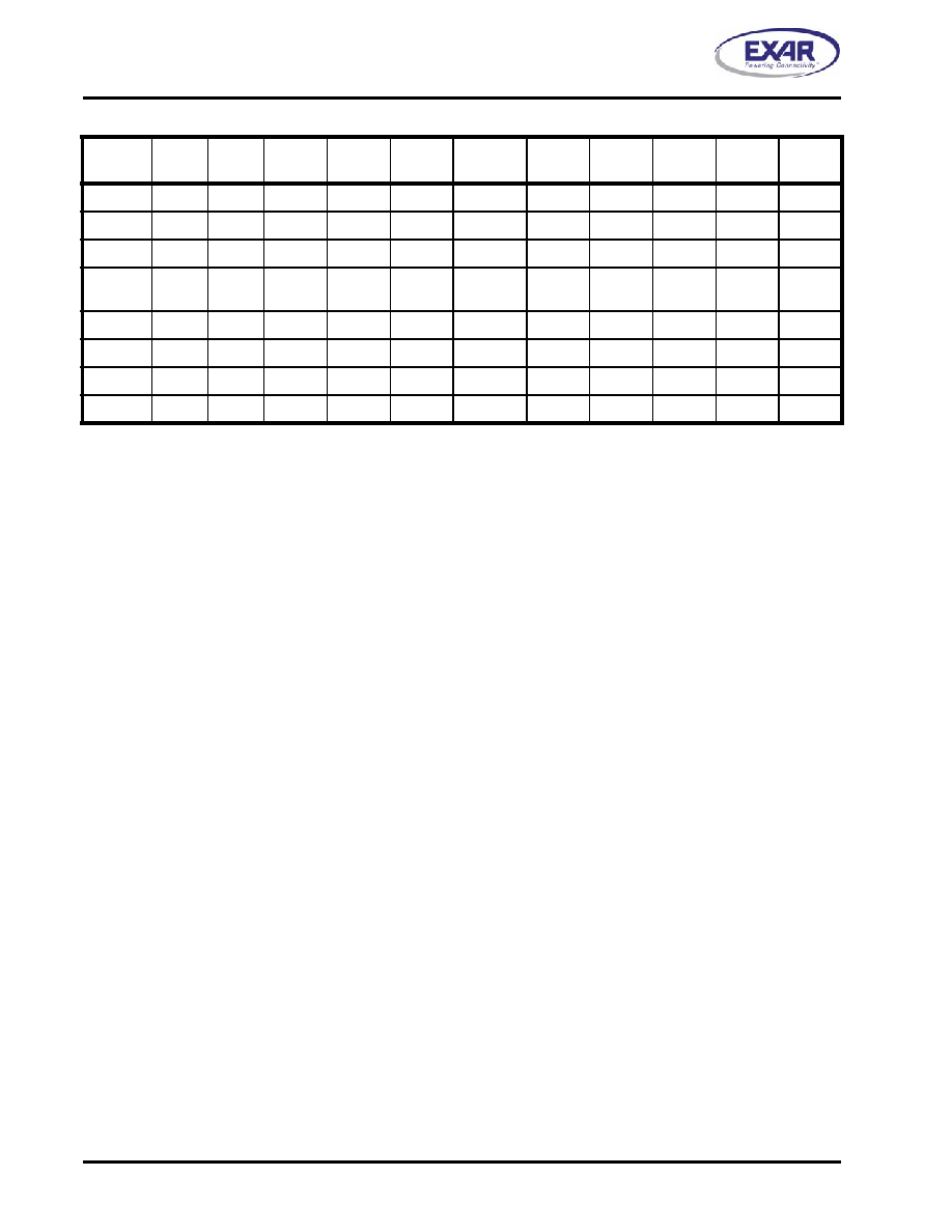
TABLE 12: UART CHANNEL CONFIGURATION REGISTERS DESCRIPTION. SHADED BITS ARE ENABLED BY EFR BIT-4.
ADDRESS
A3-A0
REG
NAME
READ/
WRITE
BIT-7
BIT-6
BIT-5
BIT-4
BIT-3
BIT-2
BIT-1
BIT-0
COMMENT
相關PDF資料 |
PDF描述 |
|---|---|
| XR16V698IQ-0B-EVB | EVAL BOARD FOR XR16V698-B 100QFP |
| XR16V698IQ-0A-EVB | EVAL BOARD FOR XR16V698-A 100QFP |
| KIT33972AEWEVBE | KIT EVALUATION FOR MC33972 |
| EBM31DCMS | CONN EDGECARD 62POS .156 WW |
| VI-J1L-EX | CONVERTER MOD DC/DC 28V 75W |
相關代理商/技術參數(shù) |
參數(shù)描述 |
|---|---|
| XR16V798IQ-0B-EVB | 功能描述:UART 接口集成電路 Supports V798 100 ld QFP,PCI Interface RoHS:否 制造商:Texas Instruments 通道數(shù)量:2 數(shù)據(jù)速率:3 Mbps 電源電壓-最大:3.6 V 電源電壓-最小:2.7 V 電源電流:20 mA 最大工作溫度:+ 85 C 最小工作溫度:- 40 C 封裝 / 箱體:LQFP-48 封裝:Reel |
| XR16V798IQ-F | 功能描述:UART 接口集成電路 UART RoHS:否 制造商:Texas Instruments 通道數(shù)量:2 數(shù)據(jù)速率:3 Mbps 電源電壓-最大:3.6 V 電源電壓-最小:2.7 V 電源電流:20 mA 最大工作溫度:+ 85 C 最小工作溫度:- 40 C 封裝 / 箱體:LQFP-48 封裝:Reel |
| XR16V798IQTR-F | 制造商:Exar Corporation 功能描述:UART 8-CH 64Byte FIFO 2.5V/3.3V 100-Pin PQFP T/R |
| XR-1790 | 制造商:未知廠家 制造商全稱:未知廠家 功能描述:Audio Schematic |
| XR17C152 | 制造商:EXAR 制造商全稱:EXAR 功能描述:5V PCI BUS DUAL UART |
發(fā)布緊急采購,3分鐘左右您將得到回復。