- 您現(xiàn)在的位置:買(mǎi)賣(mài)IC網(wǎng) > PDF目錄48109 > YSS943-VZ SPECIALTY CONSUMER CIRCUIT, PQFP144 PDF資料下載
參數(shù)資料
| 型號(hào): | YSS943-VZ |
| 元件分類(lèi): | 消費(fèi)家電 |
| 英文描述: | SPECIALTY CONSUMER CIRCUIT, PQFP144 |
| 封裝: | LEAD FREE, PLASTIC, LQFP-144 |
| 文件頁(yè)數(shù): | 6/36頁(yè) |
| 文件大?。?/td> | 831K |
| 代理商: | YSS943-VZ |
第1頁(yè)第2頁(yè)第3頁(yè)第4頁(yè)第5頁(yè)當(dāng)前第6頁(yè)第7頁(yè)第8頁(yè)第9頁(yè)第10頁(yè)第11頁(yè)第12頁(yè)第13頁(yè)第14頁(yè)第15頁(yè)第16頁(yè)第17頁(yè)第18頁(yè)第19頁(yè)第20頁(yè)第21頁(yè)第22頁(yè)第23頁(yè)第24頁(yè)第25頁(yè)第26頁(yè)第27頁(yè)第28頁(yè)第29頁(yè)第30頁(yè)第31頁(yè)第32頁(yè)第33頁(yè)第34頁(yè)第35頁(yè)第36頁(yè)
YSS944/943/940
14
(2) On-chip memory access (firmware download)
Access to on-chip memory is performed in 32-bit units via the microprocessor interface. Also, on-chip
memory access can be performed concurrently with register access. The two firmware downloading
methods prepared for this LSI are explained below.
(a) Burst transfer mode
When the IA carrier (PRGMOD[1:0] = 11) is used, instruction code/coefficient data firmware can be
downloaded in this mode. By using this mode, a large amount of data can be downloaded at high speeds
when initialization is executed or when the sampling frequency is changed. The features of the burst
transfer mode are as follows.
During the transfer period, decoding is aborted and data is transferred at high speeds. Muting is
automatically effected during the transfer period.
Data transferred from the microprocessor can be received without handshaking.
Both instruction code firmware and coefficient data firmware can be downloaded.
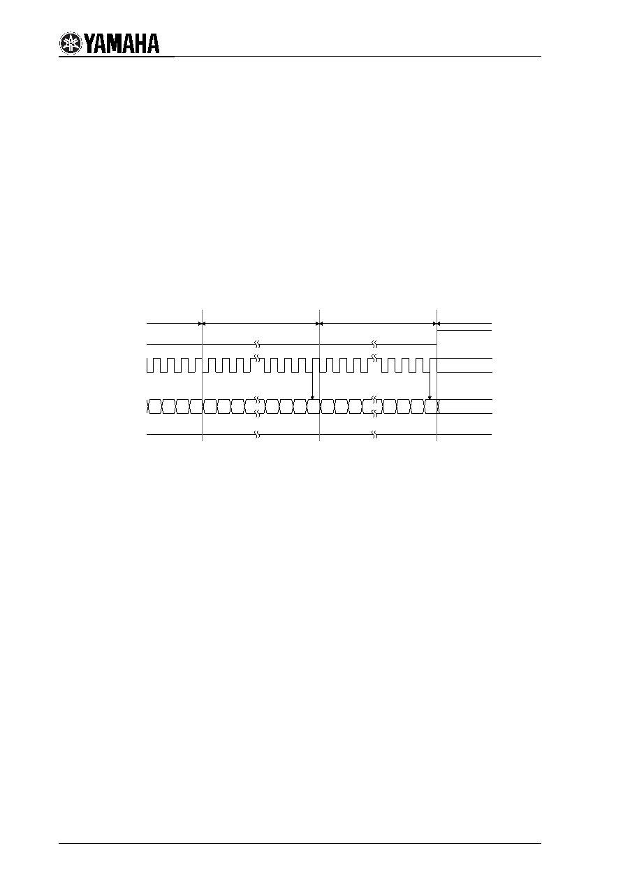
The microprocessor interface’s sequence in firmware downloading burst transfer mode is shown below.
A
D0
A
D1
A
D28
A
D29
A
D30
A
D31
High-Z
MISO
MISCK
MISI
nMICS
D6
D7
<1>
A
D2
A
D3
D4
D5
<2>
A+1
D0
A+1
D1
A+n
D28
A+1
D2
A+1
D3
<3>
A+n
D29
A+n
D30
A+n
D31
Don't care
<4>
[Access steps and statuses]
<1> Register setting:
The microprocessor interface function change for the on-chip memory access start address (A in
figure) and on-chip memory access is set by register as shown below.
Set the instruction code firmware download mode (IACNFG = 1)
Change the firmware program mode to IA carrier (PRGMOD[1:0] = 11).
Set the on-chip memory access start address IAA[20:0].
Change the function of the microprocessor interface pin from register access to on-chip memory
access (IA = 1).
Once this setting is made, the microprocessor interface functions in firmware downloading burst
transfer mode until the nMICS pin is set to high level.
<2> Start firmware download:
The nMICS pin is fixed at low level.
Data is transferred LSB first, in 32-bit units.
Data is written to on-chip memory when the rising edge of MISCK occurs for the 32nd bit of data
(D31 in the figure).
<3> Continuation and termination of firmware download:
Each time 32 bits of data are written, IAA[20:0] is automatically incremented. Accordingly, when
writing to consecutive addresses, only the data is transferred.
When nMICS changes from low level to high level, firmware download ends and the
microprocessor interface returns to accessing registers.
When accessing non-consecutive on-chip memory addresses or when resuming firmware
downloading after an access interruption, be sure to set IAA[20:0] as described in <1> above.
<4> When this LSI has not been selected:
<5> Register setting:
After completing a firmware download, perform the following processing.
Set the instruction code firmware execution mode (IACNFG = 0).
Report the existence of boot firmware to this LSI (DL = 1).
Change the firmware program mode PRGMOD[1:0] from “IA carrier” to another mode.
相關(guān)PDF資料 |
PDF描述 |
|---|---|
| YSS944-VZ | SPECIALTY CONSUMER CIRCUIT, PQFP144 |
| YSS940-VZ | SPECIALTY CONSUMER CIRCUIT, PQFP144 |
| YSS950-SZ | 0-BIT, 12.5 MHz, OTHER DSP, CQFP64 |
| YSS951-VZ | SPECIALTY CONSUMER CIRCUIT, PQFP48 |
| YTD421B-E | SPECIALTY TELECOM CIRCUIT, PDSO20 |
相關(guān)代理商/技術(shù)參數(shù) |
參數(shù)描述 |
|---|---|
| YSS944 | 制造商:YAMAHA 制造商全稱(chēng):YAMAHA CORPORATION 功能描述:ADAMB Advanced Digital Audio Multi channel decode processor |
| YSS950 | 制造商:YAMAHA 制造商全稱(chēng):YAMAHA CORPORATION 功能描述:DAP1 Digital Audio Processor |
| YST 35-22 P24 C3 | 制造商:n/a 功能描述:Thyristor Puck |
| YST025 | 制造商:YEONHO 制造商全稱(chēng):YEONHO ELECTRONICS 功能描述:2.50mm PITCH CONNECTOR |
| YST025J | 制造商:YEONHO 制造商全稱(chēng):YEONHO ELECTRONICS 功能描述:2.50mm PITCH CONNECTOR |
發(fā)布緊急采購(gòu),3分鐘左右您將得到回復(fù)。