- 您現(xiàn)在的位置:買賣IC網(wǎng) > PDF目錄373766 > Z86C46 (ZiLOG, Inc.) CMOS Z8 MCU(CMOS Z8系列微控制器) PDF資料下載
參數(shù)資料
| 型號: | Z86C46 |
| 廠商: | ZiLOG, Inc. |
| 英文描述: | CMOS Z8 MCU(CMOS Z8系列微控制器) |
| 中文描述: | 單片機的CMOS Z8的CMOS(Z8系列微控制器) |
| 文件頁數(shù): | 39/70頁 |
| 文件大小: | 1192K |
| 代理商: | Z86C46 |
第1頁第2頁第3頁第4頁第5頁第6頁第7頁第8頁第9頁第10頁第11頁第12頁第13頁第14頁第15頁第16頁第17頁第18頁第19頁第20頁第21頁第22頁第23頁第24頁第25頁第26頁第27頁第28頁第29頁第30頁第31頁第32頁第33頁第34頁第35頁第36頁第37頁第38頁當前第39頁第40頁第41頁第42頁第43頁第44頁第45頁第46頁第47頁第48頁第49頁第50頁第51頁第52頁第53頁第54頁第55頁第56頁第57頁第58頁第59頁第60頁第61頁第62頁第63頁第64頁第65頁第66頁第67頁第68頁第69頁第70頁
Z86C34/C35/C36/C44/C45/C46
CMOS Z8 MCUs with ASCI UART
ZiLOG
DS007601-Z8X0499
P R E L I M I N A R Y
39
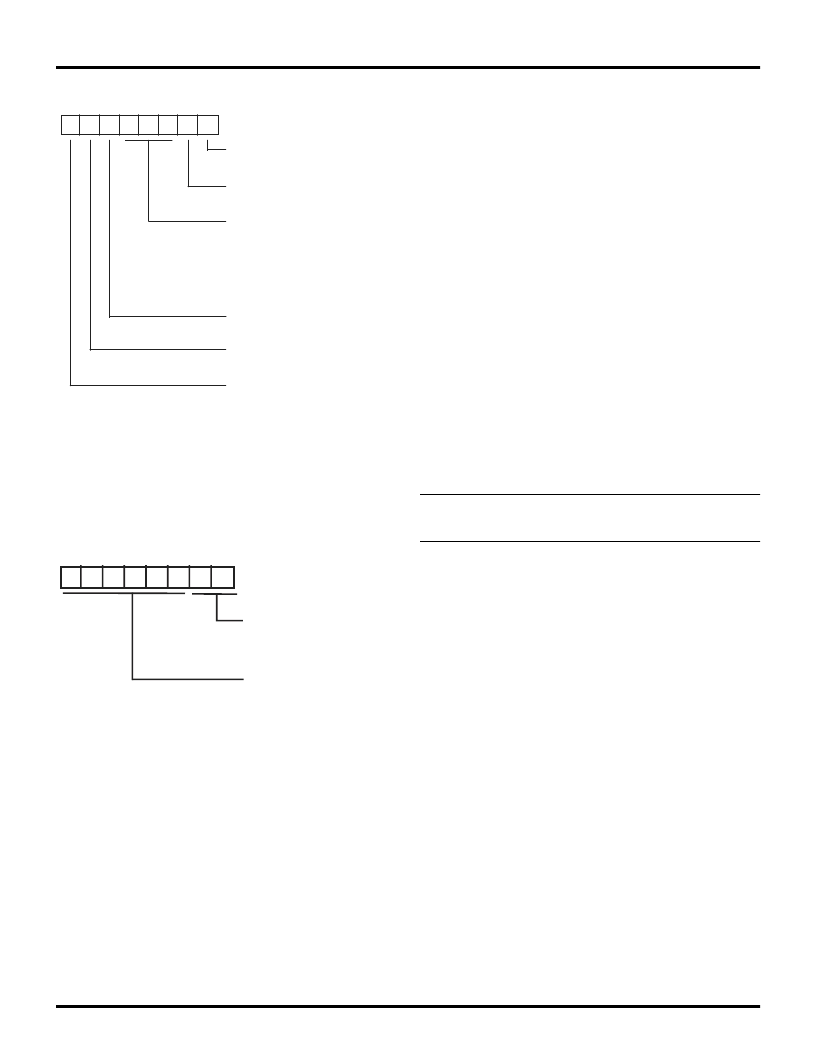
SCLK/TCLK Divide-by-16 Select (D0).
D0 of the
SMR
controls a divide-by-16 prescaler of
SCLK/TCLK
. The pur-
pose of this control is to selectively reduce device power
consumption during normal processor execution (
SCLK
control) and/or
HALT
mode (where
TCLK
sources
counter/timers and interrupt logic). This bit is reset to
D0
= 0
after a Stop-Mode Recovery.
External Clock Divide-by-Two (D1).
This bit can elimi-
nate the oscillator divide-by-two circuitry. When this bit is
0, the System Clock (
SCLK
) and Timer Clock (
TCLK
) are
equal to the external clock frequency divided by 2. The
SCLK/TCLK
is equal to the external clock frequency when
this bit is set (
D1 = 1
). Using this bit together with
D7
of
PCON
further helps lower EMI (that is,
D7
(
PCON
) = 0,
D1
(SMR) = 1
). The default setting is
0
. Maximum external
clock frequency is 4 MHz when
SMR BIT D1 = 1
where
SCLK/TCLK = XTAL
.
Stop-Mode Recovery Source (D2, D3, and D4).
These
three bits of the
SMR
specify the wake-up source of the
STOP
recovery (Figure 28 and Table 13). When the Stop-
Mode Recovery Sources are selected in this register, then
SMR2
register bits
D0
,
D1
must be set to
0
.
Note:
If the Port 2 pin is configured as an output, this output
level is read by the
SMR
circuitry.
Figure 26. Stop-Mode Recovery Register
(WRITE ONLY Except Bit D7, Which Is READ ONLY)
Figure 27. Stop-Mode Recovery Register 2
(0F) DH: WRITE ONLY
D7
D6
D5
D4
D3
D2
D1
D0
SMR (FH) 0B
SCLK/TCLK Divide-by-16
0 OFF * *
1 ON
STOP-Mode Recovery Source
000 POR Only and/or External Reset*
001 P30
010 P31
011 P32
100 P33
101 P27
110 P2 NOR 0-3
111 P2 NOR 0-7
Stop Delay
0 OFF
1 ON*
Stop Recovery Level
0 Low*
1 High
Stop Flag (Read only)
0 POR*
1 Stop Recovery
Note: Not used in conjunction with SMR2 Source
*
Default setting after RESET.
* * Default setting after RESET and STOP-Mode Recovery.
External Clock Divide by 2
0 SCLK/TCLK =XTAL/2*
1 SCLK/TCLK =XTAL
D7
D6
D5
D4
D3
D2
D1
D0
SMR2 (0F) DH
Note: Not used in conjunction with SMR Source
Stop-Mode Recovery Source 2
00 POR only*
01 AND P20,P21,P22,P23
10 AND P20,P21,P22,P23,P24,
P25,P26,P27
Reserved (Must be 0)
相關(guān)PDF資料 |
PDF描述 |
|---|---|
| Z86C40 | CMOS Z8 CONSUMER CONTROLLER PROCESSOR |
| Z86C30 | CMOS Z8 CONSUMER CONTROLLER PROCESSOR |
| Z86C31 | CMOS Z8 CONSUMER CONTROLLER PROCESSOR |
| Z86C32 | CMOS Z8 CONSUMER CONTROLLER PROCESSOR |
| Z86C47 | CMOS Z8 MICROCONTROLLER |
相關(guān)代理商/技術(shù)參數(shù) |
參數(shù)描述 |
|---|---|
| Z86C47 | 制造商:ZILOG 制造商全稱:ZILOG 功能描述:CMOS Z8 MICROCONTROLLER |
| Z86C4704PSC | 制造商:未知廠家 制造商全稱:未知廠家 功能描述:8-Bit Microcontroller |
| Z86C5000ZEM | 功能描述:仿真器/模擬器 Z8 In-Circuit Em-C50 RoHS:否 制造商:Blackhawk 產(chǎn)品:System Trace Emulators 工具用于評估:C6000, C5000, C2000, OMAP, DAVINCI, SITARA, TMS470, TMS570, ARM 7/9, ARM Cortex A8/R4/M3 用于:XDS560v2 |
| Z86C50-20GSE | 制造商:未知廠家 制造商全稱:未知廠家 功能描述:8-Bit Microcontroller |
| Z86C50-20VSC | 制造商:未知廠家 制造商全稱:未知廠家 功能描述:Microcontroller |
發(fā)布緊急采購,3分鐘左右您將得到回復(fù)。