- 您現(xiàn)在的位置:買賣IC網(wǎng) > PDF目錄373771 > Z8S18033FEC (ZILOG INC) ENHANCED Z180 MICROPROCESSOR PDF資料下載
參數(shù)資料
| 型號: | Z8S18033FEC |
| 廠商: | ZILOG INC |
| 元件分類: | 微控制器/微處理器 |
| 英文描述: | ENHANCED Z180 MICROPROCESSOR |
| 中文描述: | 8-BIT, MICROPROCESSOR, PQFP80 |
| 封裝: | QFP-80 |
| 文件頁數(shù): | 40/70頁 |
| 文件大小: | 387K |
| 代理商: | Z8S18033FEC |
第1頁第2頁第3頁第4頁第5頁第6頁第7頁第8頁第9頁第10頁第11頁第12頁第13頁第14頁第15頁第16頁第17頁第18頁第19頁第20頁第21頁第22頁第23頁第24頁第25頁第26頁第27頁第28頁第29頁第30頁第31頁第32頁第33頁第34頁第35頁第36頁第37頁第38頁第39頁當(dāng)前第40頁第41頁第42頁第43頁第44頁第45頁第46頁第47頁第48頁第49頁第50頁第51頁第52頁第53頁第54頁第55頁第56頁第57頁第58頁第59頁第60頁第61頁第62頁第63頁第64頁第65頁第66頁第67頁第68頁第69頁第70頁
Z80180/Z8S180/Z8L180
Enhanced Z180 Microprocessor
Zilog
1-40
P R E L I M I N A R Y
DS971800401
MOD2, 1, 0: ASCI Data Format Mode 2, 1, 0 (bits 2-0).
These bits program the ASCI data format as follows.
MOD2
= 0
→
7
bit data
= 1
→
8 bit data
MOD1
= 0
→
No parity
= 1
→
Parity enabled
MOD0
= 0
→
1 stop bit
= 1
→
2 stop bits
The data formats available based on all combinations of
MOD2, MOD1, and MOD0 are shown in Table 5-6.
ASCI CHANNEL CONTROL REGISTER B
MPBT: Multiprocessor Bit Transmit (bit 7).
When multi-
processor communication format is selected (MP bit = 1),
MPBT is used to specify the MPB data bit for transmission.
If MPBT = 1, then MPB = 1 is transmitted. If MPBT = 0,
then MPB = 0 is transmitted. MPBT state is undefined dur-
ing and after RESET.
MP: Multiprocessor Mode (bit 6).
When MP is set to 1,
the data format is configured for multiprocessor mode
based on the MOD2 (number of data bits) and MOD0
(number of stop bits) bits in CNTLA. The format is as fol-
lows.
Start bit + 7 or 8 data bits + MPB bit + 1 or 2 stop bits
Note that multiprocessor (MP=1) format has no provision
for parity. If MP = 0, the data format is based on MOD0,
MOD1, MOD2, and may include parity. The MP bit is
cleared to 0 during RESET.
CTS/PS: Clear to Send/Prescale (bit 5).
When read,
/CTS/PS reflects the state of the external /CTS input. If the
/CTS input pin is HIGH, /CTS/PS will be read as 1. Note
that when the /CTS input pin is HIGH, the TDRE bit is in-
hibited (i.e. held at 0). For channel 1, the /CTS input is mul-
tiplexed with RXS pin (Clocked Serial Receive Data).
Thus, /CTS/PS is only valid when read if the channel 1
CTS1E bit = 1 and the /CTS input pin function is selected.
The read data of /CTS/PS is not affected by RESET.
If the SS2-0 bits in this register are not 111, and the BRG
mode bit in the ASEXT register is 0, then writing to this bit
sets the prescale (PS) control as described in the following
“Clock Modes” section. Under those circumstances, a 0 in-
dicates a divide by 10 prescale function while a 1 indicates
divide by 30. The bit resets to 0.
PEO: Parity Even Odd (bit 4).
PEO selects oven or odd
parity. PEO does not affect the enabling/disabling of parity
(MOD1 bit of CNTLA). If PEO is cleared to 0, even parity
is selected. If PEO is set to 1, odd parity is selected. PEO
is cleared to 0 during RESET.
DR: Divide Ratio (bit 3).
If the X1 bit in the ASEXT regis-
ter is 0, this bit specifies the divider used to obtain baud
rate from the data sampling clock. If DR is reset to 0, di-
vide- by-16 is used, while if DR is set to 1 divide-by-64 is
used. DR is cleared to 0 during RESET.
SS2,1,0: Source/Speed Select 2,1,0 (bits 2-0).
First, if
these bits are 111, as they are after a Reset, the CKA pin
Table 5. Data Formats
MOD2 MOD1 MOD0 Data Format
0
0
0
0
0
1
0
1
1
0
1
0
1
1
1
1
0
1
0
1
0
1
0
1
Start + 7 bit data + 1 stop
Start + 7 bit data + 2 stop
Start + 7 bit data + parity + 1 stop
Start + 7 bit data + parity + 2 stop
Start + 8 bit data + 1 stop
Start + 8 bit data + 2 stop
Start + 8 bit data + parity + 1 stop
Start + 8 bit data + parity + 2 stop
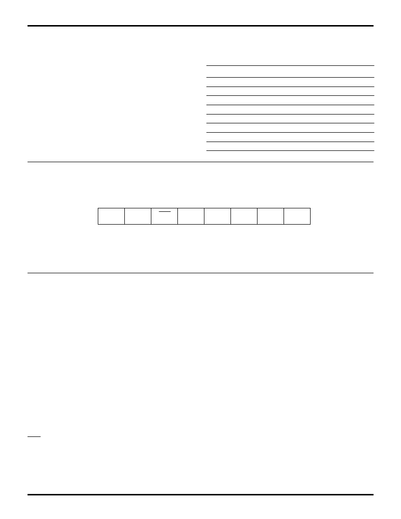
Figure 34. ASCI Channel Control Register B
Bit
MPBT
MP
R/W
R/W
R/W
CTS/
PS
7
6
5
4
3
2
1
0
PEO
DR
SS2
SS1
SS0
R/W
R/W
ASCI Control Register B 1 (CNTLB1: I/O Address = 03H)
R/W
R/W
R/W
ASCI Control Register B 0 (CNTLB0: I/O Address = 02H)
相關(guān)PDF資料 |
PDF描述 |
|---|---|
| Z8S18033FSC | CONN POWER HEADER 5ROW 10POS P-F |
| Z8S18033PEC | ENHANCED Z180 MICROPROCESSOR |
| Z8S18033PSC | ENHANCED Z180 MICROPROCESSOR |
| Z8S18033VEC | CONN HDR INVERSE 30POS 5ROW R/A |
| Z8S18033VSC | CONN HDR INVERSE 120POS 5ROW R/A |
相關(guān)代理商/技術(shù)參數(shù) |
參數(shù)描述 |
|---|---|
| Z8S18033FEC00TR | 功能描述:IC Z180 MPU 80QFP RoHS:否 類別:集成電路 (IC) >> 嵌入式 - 微處理器 系列:Z180 標(biāo)準(zhǔn)包裝:40 系列:MPC83xx 處理器類型:32-位 MPC83xx PowerQUICC II Pro 特點:- 速度:267MHz 電壓:0.95 V ~ 1.05 V 安裝類型:表面貼裝 封裝/外殼:516-BBGA 裸露焊盤 供應(yīng)商設(shè)備封裝:516-PBGAPGE(27x27) 包裝:托盤 |
| Z8S18033FEG | 功能描述:微處理器 - MPU 33MHz STATIC Z180 XT RoHS:否 制造商:Atmel 處理器系列:SAMA5D31 核心:ARM Cortex A5 數(shù)據(jù)總線寬度:32 bit 最大時鐘頻率:536 MHz 程序存儲器大小:32 KB 數(shù)據(jù) RAM 大小:128 KB 接口類型:CAN, Ethernet, LIN, SPI,TWI, UART, USB 工作電源電壓:1.8 V to 3.3 V 最大工作溫度:+ 85 C 安裝風(fēng)格:SMD/SMT 封裝 / 箱體:FBGA-324 |
| Z8S18033FSC | 功能描述:微處理器 - MPU 33MHz STATIC Z180 RoHS:否 制造商:Atmel 處理器系列:SAMA5D31 核心:ARM Cortex A5 數(shù)據(jù)總線寬度:32 bit 最大時鐘頻率:536 MHz 程序存儲器大小:32 KB 數(shù)據(jù) RAM 大小:128 KB 接口類型:CAN, Ethernet, LIN, SPI,TWI, UART, USB 工作電源電壓:1.8 V to 3.3 V 最大工作溫度:+ 85 C 安裝風(fēng)格:SMD/SMT 封裝 / 箱體:FBGA-324 |
| Z8S18033FSC00TR | 功能描述:IC Z180 MPU 80QFP RoHS:否 類別:集成電路 (IC) >> 嵌入式 - 微處理器 系列:Z180 標(biāo)準(zhǔn)包裝:40 系列:MPC83xx 處理器類型:32-位 MPC83xx PowerQUICC II Pro 特點:- 速度:267MHz 電壓:0.95 V ~ 1.05 V 安裝類型:表面貼裝 封裝/外殼:516-BBGA 裸露焊盤 供應(yīng)商設(shè)備封裝:516-PBGAPGE(27x27) 包裝:托盤 |
| Z8S18033FSG | 功能描述:微處理器 - MPU 33MHz STATIC Z180 RoHS:否 制造商:Atmel 處理器系列:SAMA5D31 核心:ARM Cortex A5 數(shù)據(jù)總線寬度:32 bit 最大時鐘頻率:536 MHz 程序存儲器大小:32 KB 數(shù)據(jù) RAM 大小:128 KB 接口類型:CAN, Ethernet, LIN, SPI,TWI, UART, USB 工作電源電壓:1.8 V to 3.3 V 最大工作溫度:+ 85 C 安裝風(fēng)格:SMD/SMT 封裝 / 箱體:FBGA-324 |
發(fā)布緊急采購,3分鐘左右您將得到回復(fù)。