- 您現(xiàn)在的位置:買賣IC網(wǎng) > PDF目錄373781 > ZL10038LDG (Zarlink Semiconductor Inc.) MULTIMETER, DIGITAL; Accuracy, AC voltage range:+/-1.5% rdg + 3 digits; Accuracy, DC current range:+/-2.5% rdg + 3 digits; Accuracy, DC voltage range:+/-1.2% rdg + 3 digits; Accuracy, resistance range:+/-1.5%rdg + 3 digits; Current RoHS Compliant: NA PDF資料下載
參數(shù)資料
| 型號(hào): | ZL10038LDG |
| 廠商: | Zarlink Semiconductor Inc. |
| 英文描述: | MULTIMETER, DIGITAL; Accuracy, AC voltage range:+/-1.5% rdg + 3 digits; Accuracy, DC current range:+/-2.5% rdg + 3 digits; Accuracy, DC voltage range:+/-1.2% rdg + 3 digits; Accuracy, resistance range:+/-1.5%rdg + 3 digits; Current RoHS Compliant: NA |
| 中文描述: | 數(shù)字衛(wèi)星調(diào)諧器射頻旁路 |
| 文件頁數(shù): | 25/38頁 |
| 文件大?。?/td> | 939K |
| 代理商: | ZL10038LDG |
第1頁第2頁第3頁第4頁第5頁第6頁第7頁第8頁第9頁第10頁第11頁第12頁第13頁第14頁第15頁第16頁第17頁第18頁第19頁第20頁第21頁第22頁第23頁第24頁當(dāng)前第25頁第26頁第27頁第28頁第29頁第30頁第31頁第32頁第33頁第34頁第35頁第36頁第37頁第38頁
ZL10036
Data Sheet
25
Zarlink Semiconductor Inc.
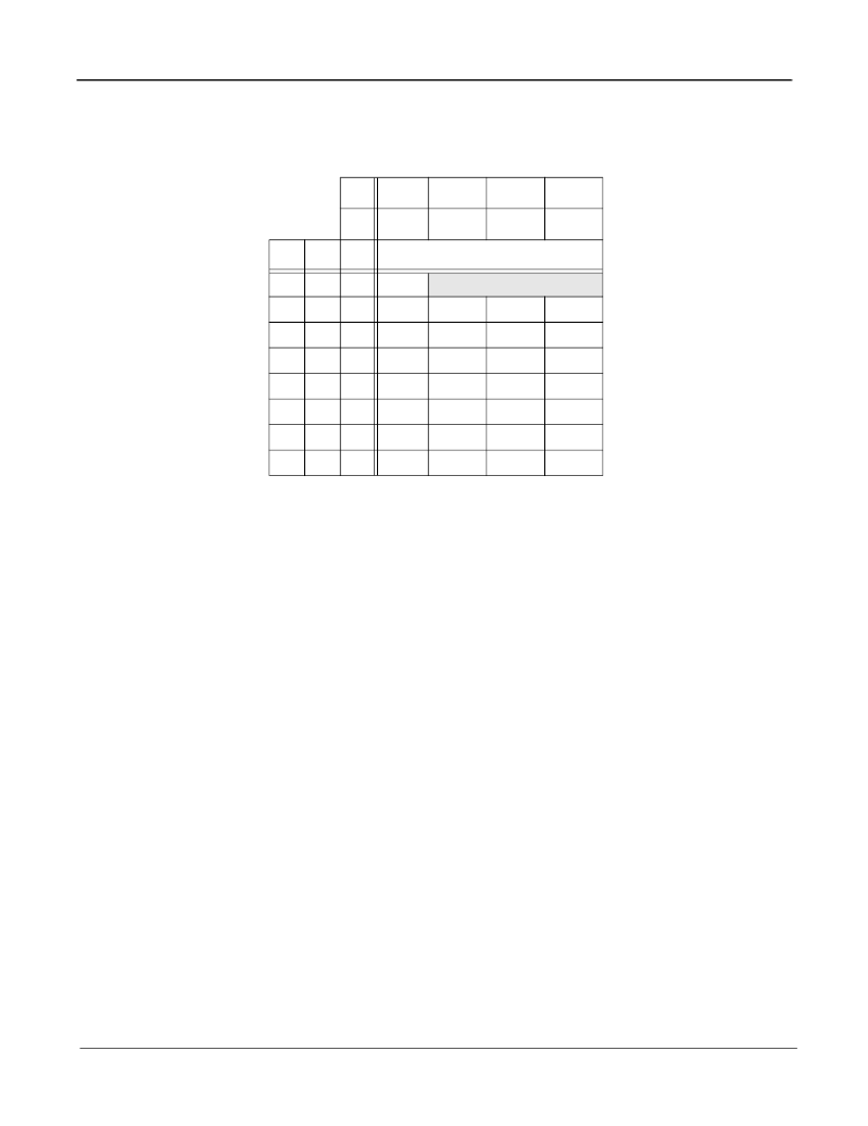
3.4.12 Reference Division Ratios (R4:0 Bits)
Register bits
R4:0
control the reference divider ratios as shown in Table 13. They are programmed through bit-4 to
bit-0 respectively, in byte-5.
3.4.13 Baseband Filter Resistor Switching (RSD)
The baseband filters use a resistor switching technique that improves bandwidth and phase matching between the
I and Q channels. The bandwidth range is effectively separated into 3 sub-ranges with different resistor values
being used in each sub-range. It is possible for the filter bandwidth accuracy to be degraded if the bandwidth setting
happens to coincide with one of the two transition points between these regions. This can be overcome by disabling
the resistor switching using the
RSD
bit. For optimum filter performance the
RSD
bit should first be enabled so that
the correct resistor value is automatically set for the selected bandwidth.
The
RSD
bit (bit-3 of byte-6) controls the resistor switching. With the default setting of logic '0' it is enabled and the
correct resistor value automatically chosen. With the
RSD
bit set to a logic '1' then the switching is disabled and this
freezes the resistors at their chosen value. The procedure when selecting a new bandwidth setting is to enable then
disable the switching; set
RSD
to logic '0' then to logic '1'.
3.4.14 Baseband Filter Bandwidth (BF6:1 & BR4:0 Bits)
Bits 6 to 1 of byte-7 configure bits
BF6
to
BF1
respectively. These bits set a decimal number in the range 0 to 62
(63 is not allowed) to determine the baseband filter bandwidth in conjunction with other values.
Bits 6 to 2 of byte-13 configure bits
BR4
to
BR0
respectively. These bits set the reference divider ratio for the
baseband filter. A number in the range 4 to 27 inclusive (values outside this range are not allowed) can be set, with
the proviso that the value of f
xtal
/BR4:0 must also be in the range 575 kHz to 2,500 kHz.
For further details, please also see 2.4, “Baseband Filter“ on page 17 and “Symbol Rate and Filter Calculations”
(sect. 4.3) on page 26.
3.4.15 LO Test (TL Bit)
For test purposes, the LO clock divided by the prescaler ratio can be output on the LOTEST pin by setting bit
TL
(byte-13 bit-0) to a logic ‘1’. By default this output is off, i.e., the
TL
bit is at logic ‘0’.
R4
0
0
1
1
R3
0
1
0
1
R2
R1
R0
Division Ratios
0
0
0
2
Illegal states
0
0
1
4
5
6
7
0
1
0
8
10
12
14
0
1
1
16
20
24
28
1
0
0
32
40
48
56
1
0
1
64
80
96
112
1
1
0
128
160
192
224
1
1
1
256
320
384
448
Table 13 - Division Ratios Set with Bits R4 - R0
相關(guān)PDF資料 |
PDF描述 |
|---|---|
| ZL10036 | Digital Satellite Tuner with RF Bypass |
| ZL10036LDF | Digital Satellite Tuner with RF Bypass |
| ZL10036LDF1 | Digital Satellite Tuner with RF Bypass |
| ZL10036LDG | Digital Satellite Tuner with RF Bypass |
| ZL10036LDG1 | Digital Satellite Tuner with RF Bypass |
相關(guān)代理商/技術(shù)參數(shù) |
參數(shù)描述 |
|---|---|
| ZL10039 | 制造商:ZARLINK 制造商全稱:Zarlink Semiconductor Inc 功能描述:Digital Satellite Tuner with RF Bypass |
| ZL10039LCF | 制造商:ZARLINK 制造商全稱:Zarlink Semiconductor Inc 功能描述:Digital Satellite Tuner with RF Bypass |
| ZL10039LCF1 | 制造商:ZARLINK 制造商全稱:Zarlink Semiconductor Inc 功能描述:Digital Satellite Tuner with RF Bypass |
| ZL10039LCG | 制造商:ZARLINK 制造商全稱:Zarlink Semiconductor Inc 功能描述:Digital Satellite Tuner with RF Bypass |
| ZL10039LCG1 | 制造商:ZARLINK 制造商全稱:Zarlink Semiconductor Inc 功能描述:Digital Satellite Tuner with RF Bypass |
發(fā)布緊急采購,3分鐘左右您將得到回復(fù)。