- 您現(xiàn)在的位置:買賣IC網(wǎng) > PDF目錄67320 > 5962-0051901NXD (TEXAS INSTRUMENTS INC) 2-CH 12-BIT PROPRIETARY METHOD ADC, PARALLEL ACCESS, PDSO32 PDF資料下載
參數(shù)資料
| 型號: | 5962-0051901NXD |
| 廠商: | TEXAS INSTRUMENTS INC |
| 元件分類: | ADC |
| 英文描述: | 2-CH 12-BIT PROPRIETARY METHOD ADC, PARALLEL ACCESS, PDSO32 |
| 封裝: | PLASTIC, TSSOP-32 |
| 文件頁數(shù): | 1/42頁 |
| 文件大小: | 840K |
| 代理商: | 5962-0051901NXD |
當前第1頁第2頁第3頁第4頁第5頁第6頁第7頁第8頁第9頁第10頁第11頁第12頁第13頁第14頁第15頁第16頁第17頁第18頁第19頁第20頁第21頁第22頁第23頁第24頁第25頁第26頁第27頁第28頁第29頁第30頁第31頁第32頁第33頁第34頁第35頁第36頁第37頁第38頁第39頁第40頁第41頁第42頁

THS12082
12-BIT, 8 MSPS, SIMULTANEOUS SAMPLING ANALOG-TO-DIGITAL CONVERTERS
SLAS271B – MAY 2000 – REVISED DECEMBER 2002
1
POST OFFICE BOX 655303
DALLAS, TEXAS 75265
features
D Simultaneous Sampling of 2 Single-Ended
Signals or 1 Differential Signal
D Integrated 16 Word FIFO
D Signal-to-Noise and Distortion Ratio: 66 dB
at fI = 2 MHz
D Differential Nonlinearity Error: ±1 LSB
D Integral Nonlinearity Error: ±1.5 LSB
D Auto-Scan Mode for 2 Inputs
D 3-V or 5-V Digital Interface Compatible
D Low Power: 216 mW Max
D 5-V Analog Single Supply Operation
D Internal Voltage References . . . 50 PPM/°C
and
±5% Accuracy
D Parallel C/DSP Interface
applications
D Radar Applications
D Communications
D Control Applications
D High-Speed DSP Front-End
D Automotive Applications
description
The THS12082 is a CMOS, low-power, 12-bit, 8 MSPS analog-to-digital converter (ADC). The speed,
resolution, bandwidth, and single-supply operation are suited for applications in radar, imaging, high-speed
acquisition, and communications. A multistage pipelined architecture with output error correction logic provides
for no missing codes over the full operating temperature range. Internal control registers allow for programming
the ADC into the desired mode. The THS12082 consists of two analog inputs, which are sampled
simultaneously. These inputs can be selected individually and configured to single-ended or differential inputs.
An integrated 16 word deep FIFO allows the storage of data in order to take the load off of the processor
connected to the ADC. Internal reference voltages for the ADC (1.5 V and 3.5 V) are provided.
An external reference can also be chosen to suit the dc accuracy and temperature drift requirements of the
application. Two different conversion modes can be selected. In the single conversion mode, a single and
simultaneous conversion can be initiated by using the single conversion start signal (CONVST). The conversion
clock in the single conversion mode is generated internally using a clock oscillator circuit. In the continuous
conversion mode, an external clock signal is applied to the CONV_CLK input of the THS12082. The internal
clock oscillator is switched off in the continuous conversion mode.
The THS12082C is characterized for operation from 0
°C to 70°C, and the THS12082I is characterized for
operation from –40
°C to 85°C.
Copyright
2002, Texas Instruments Incorporated
PRODUCTION DATA information is current as of publication date.
Products conform to specifications per the terms of Texas Instruments
standard warranty. Production processing does not necessarily include
testing of all parameters.
Please be aware that an important notice concerning availability, standard warranty, and use in critical applications of
Texas Instruments semiconductor products and disclaimers thereto appears at the end of this data sheet.
1
2
3
4
5
6
7
8
9
10
11
12
13
14
15
16
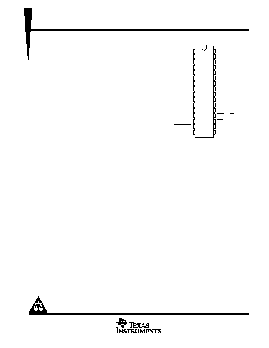
32
31
30
29
28
27
26
25
24
23
22
21
20
19
18
17
D0
D1
D2
D3
D4
D5
BVDD
BGND
D6
D7
D8
D9
RA0/D10
RA1/D11
CONV_CLK (CONVST)
DATA_AV
OV_FL
RESET
AINP
AINM
REFIN
REFOUT
REFP
REFM
AGND
AVDD
CS0
CS1
WR (R/W)
RD
DVDD
DGND
DA PACKAGE
(TOP VIEW)
相關(guān)PDF資料 |
PDF描述 |
|---|---|
| THS12082IDA | 2-CH 12-BIT PROPRIETARY METHOD ADC, PARALLEL ACCESS, PDSO32 |
| THS12082IDAR | 2-CH 12-BIT PROPRIETARY METHOD ADC, PARALLEL ACCESS, PDSO32 |
| THS12082CDARG4 | 2-CH 12-BIT PROPRIETARY METHOD ADC, PARALLEL ACCESS, PDSO32 |
| THS12082IDAG4 | 2-CH 12-BIT PROPRIETARY METHOD ADC, PARALLEL ACCESS, PDSO32 |
| THS12082CDAR | 2-CH 12-BIT PROPRIETARY METHOD ADC, PARALLEL ACCESS, PDSO32 |
相關(guān)代理商/技術(shù)參數(shù) |
參數(shù)描述 |
|---|---|
| 5962-0052201HXA | 制造商:未知廠家 制造商全稱:未知廠家 功能描述:DC to DC Converter |
| 5962-0052201HXC | 制造商:未知廠家 制造商全稱:未知廠家 功能描述:DC to DC Converter |
| 5962-0052201HYA | 制造商:未知廠家 制造商全稱:未知廠家 功能描述:DC to DC Converter |
| 5962-0052201HYC | 制造商:未知廠家 制造商全稱:未知廠家 功能描述:DC to DC Converter |
| 5962-0052201HZA | 制造商:未知廠家 制造商全稱:未知廠家 功能描述:DC to DC Converter |
發(fā)布緊急采購,3分鐘左右您將得到回復(fù)。