- 您現(xiàn)在的位置:買賣IC網(wǎng) > PDF目錄378210 > 80960CF (Intel Corp.) 32-Bit High-Performance Superscalar Processor(32位高性能超標量處理器) PDF資料下載
參數(shù)資料
| 型號: | 80960CF |
| 廠商: | Intel Corp. |
| 英文描述: | 32-Bit High-Performance Superscalar Processor(32位高性能超標量處理器) |
| 中文描述: | 32位高性能超標量處理器(32位高性能超標量處理器) |
| 文件頁數(shù): | 25/62頁 |
| 文件大小: | 999K |
| 代理商: | 80960CF |
第1頁第2頁第3頁第4頁第5頁第6頁第7頁第8頁第9頁第10頁第11頁第12頁第13頁第14頁第15頁第16頁第17頁第18頁第19頁第20頁第21頁第22頁第23頁第24頁當前第25頁第26頁第27頁第28頁第29頁第30頁第31頁第32頁第33頁第34頁第35頁第36頁第37頁第38頁第39頁第40頁第41頁第42頁第43頁第44頁第45頁第46頁第47頁第48頁第49頁第50頁第51頁第52頁第53頁第54頁第55頁第56頁第57頁第58頁第59頁第60頁第61頁第62頁
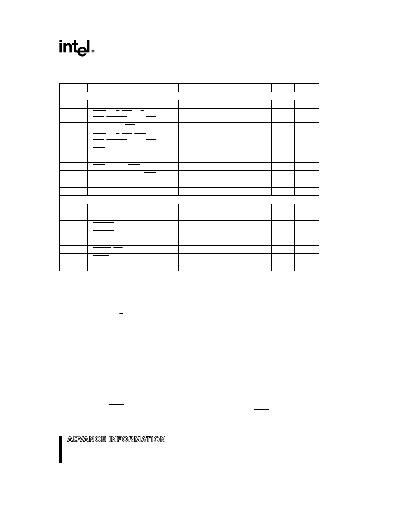
SPECIAL ENVIRONMENT 80960CF-30, -25, -16
AC Characteristics D 80960CF-30
(80960CF-30 only, under the conditions described in
Section 4.2, Operating Conditions
and
Section 4.5.1,
AC Test Conditions
.) See notes which follow this table. (Continued)
Symbol
Parameter
Min
Max
Units
Notes
RELATIVE OUTPUT TIMINGS
(9,7)
T
AVSH1
A31:2 Valid to ADS Rising
T
b
4
T
a
4
ns
T
AVSH2
BE3:0, W/R, SUP, D/C,
DMA, DACK3:0 Valid to ADS Rising
T
b
6
T
b
4
T
a
6
T
a
4
ns
T
AVEL1
A31:2 Valid to DEN Falling
ns
T
AVEL2
BE3:0, W/R, SUP, INST,
DMA, DACK3:0 Valid to DEN Falling
T
b
6
T
a
6
ns
T
NLQV
WAIT Falling to Output Data Valid
g
6
ns
T
DVNH
Output Data Valid to WAIT Rising
N
*
T
b
6
N
*
T
a
6
ns
(4)
T
NLNH
WAIT Falling to WAIT Rising
N
*
T
g
4
ns
(4)
T
NHQX
Output Data Hold after WAIT Rising
(N
a
1)
*
T
b
6
T/2
b
6
T/2
b
4
(N
a
1)
*
T
a
6
%
T/2
a
4
ns
(5)
T
EHTV
DT/R Hold after DEN High
ns
(6)
T
TVEL
RELATIVE INPUT TIMINGS
(7)
DT/R Valid to DEN Falling
ns
(7)
T
IS5
RESET Input Setup (2x Clock Mode)
6
ns
(14)
T
IH5
RESET Input Hold (2x Clock Mode)
5
ns
(14)
T
IS6
DREQ3:0 Input Setup
12
ns
(8)
T
IH6
DREQ3:0 Input Hold
7
ns
(8)
T
IS7
XINT7:0, NMI Input Setup
7
ns
(8)
T
IH7
XINT7:0, NMI Input Hold
3
ns
(8)
T
IS8
RESET Input Setup (1x Clock Mode)
3
ns
(15)
T
IH8
RESET Input Hold (1x Clock Mode)
T/4
a
1
ns
(15)
NOTES:
1. See
Section 4.5.2, AC Timing Waveforms
for waveforms and definitions.
2. See Figure 22 for capacitive derating information for output delays and hold times.
3. See Figure 23 for capacitive derating information for rise and fall times.
4. Where N is the number of N
RAD
, N
RDD
, N
WAD
, or N
WDD
wait states that are programmed in the Bus Controller Region
Table. When there are no wait states in an access, WAIT never goes active.
5. N
e
Number of wait states inserted with READY.
6. Output Data and/or DT/R may be driven indefinitely following a cycle if there is no subsequent bus activity.
7. See Notes 1, 2 and 3.
8. Since asynchronous inputs are synchronized internally by the 80960CF they have no required setup or hold times in order
to be recognized and for proper operation. However, to guarantee recognition of the input at a particular edge of PCLK2:1
the setup times shown must be met. Asynchronous inputs must be active for at least two consecutive PCLK2:1 rising
edges to be seen by the processor.
9. These specifications are guaranteed by the processor.
10. These specifications must be met by the system for proper operation of the processor.
11. This timing is dependent upon the loading of PCLK2:1. Use the derating curves of
Section 4.5.3
to adjust the timing for
PCLK2:1 loading.
12. In the 1-x input clock mode, the maximum input clock period is limited to 125 ns while the processor is operating. When
the processor is in reset, the input clock may stop even in 1-x mode.
13. When in the 1-x input clock mode, these specifications assume a stable input clock with a period variation of less than
g
0.1% between adjacent cycles.
14. In 2x clock mode, RESET is an asynchronous input which has no required setup and hold time for proper operation.
However, to guarantee the device exits reset synchronized to a particular clock edge, the RESET pin must meet setup
and hold times to the falling edge of the CLKIN. (See Figure 28a.)
15. In 1x clock mode, RESET is an asynchronous input which has no required setup and hold time for proper operation.
However, to guarantee the device exits reset synchronized to a particular clock edge, the RESET pin must be deasserted
while CLKIN is high and meet setup and hold times to the rising edge of the CLKIN. (See Figure 28b.)
25
相關PDF資料 |
PDF描述 |
|---|---|
| 80960JD | EMBEDDED 32-BIT MICROPROCESSOR |
| 80960JT | EMBEDDED 32-BIT MICROPROCESSOR |
| 80960JF | 3.3 V EMBEDDED 32-BIT MICROPROCESSOR |
| 80960 | 3.3 V EMBEDDED 32-BIT MICROPROCESSOR |
| 80960CA-16 | SPECIAL ENVIRONMENT 80960CA-25, -16 32-BIT HIGH-PERFORMANCE EMBEDDED PROCESSOR |
相關代理商/技術參數(shù) |
參數(shù)描述 |
|---|---|
| 80960CF-16 | 制造商:INTEL 制造商全稱:Intel Corporation 功能描述:80960CF-40, -33, -25, -16 32-BIT HIGH-PERFORMANCE SUPERSCALAR EMBEDDED MICROPROCESSOR |
| 80960CF-25 | 制造商:INTEL 制造商全稱:Intel Corporation 功能描述:80960CF-40, -33, -25, -16 32-BIT HIGH-PERFORMANCE SUPERSCALAR EMBEDDED MICROPROCESSOR |
| 80960CF-30 | 制造商:INTEL 制造商全稱:Intel Corporation 功能描述:SPECIAL ENVIRONMENT 80960CF-30, -25, -16 32-BIT HIGH-PERFORMANCE SUPERSCALAR PROCESSOR |
| 80960CF-33 | 制造商:INTEL 制造商全稱:Intel Corporation 功能描述:80960CF-40, -33, -25, -16 32-BIT HIGH-PERFORMANCE SUPERSCALAR EMBEDDED MICROPROCESSOR |
| 80960CF-40 | 制造商:INTEL 制造商全稱:Intel Corporation 功能描述:80960CF-40, -33, -25, -16 32-BIT HIGH-PERFORMANCE SUPERSCALAR EMBEDDED MICROPROCESSOR |
發(fā)布緊急采購,3分鐘左右您將得到回復。