- 您現(xiàn)在的位置:買賣IC網(wǎng) > PDF目錄378211 > 80960RN (Intel Corp.) 80960RN I/O Processor(80960RN I/O 處理器) PDF資料下載
參數(shù)資料
| 型號(hào): | 80960RN |
| 廠商: | Intel Corp. |
| 英文描述: | 80960RN I/O Processor(80960RN I/O 處理器) |
| 中文描述: | 80960RN I / O處理器(80960RN的I / O處理器) |
| 文件頁(yè)數(shù): | 17/54頁(yè) |
| 文件大小: | 851K |
| 代理商: | 80960RN |
第1頁(yè)第2頁(yè)第3頁(yè)第4頁(yè)第5頁(yè)第6頁(yè)第7頁(yè)第8頁(yè)第9頁(yè)第10頁(yè)第11頁(yè)第12頁(yè)第13頁(yè)第14頁(yè)第15頁(yè)第16頁(yè)當(dāng)前第17頁(yè)第18頁(yè)第19頁(yè)第20頁(yè)第21頁(yè)第22頁(yè)第23頁(yè)第24頁(yè)第25頁(yè)第26頁(yè)第27頁(yè)第28頁(yè)第29頁(yè)第30頁(yè)第31頁(yè)第32頁(yè)第33頁(yè)第34頁(yè)第35頁(yè)第36頁(yè)第37頁(yè)第38頁(yè)第39頁(yè)第40頁(yè)第41頁(yè)第42頁(yè)第43頁(yè)第44頁(yè)第45頁(yè)第46頁(yè)第47頁(yè)第48頁(yè)第49頁(yè)第50頁(yè)第51頁(yè)第52頁(yè)第53頁(yè)第54頁(yè)
Data Sheet
—
80960RN
Advance Information
17
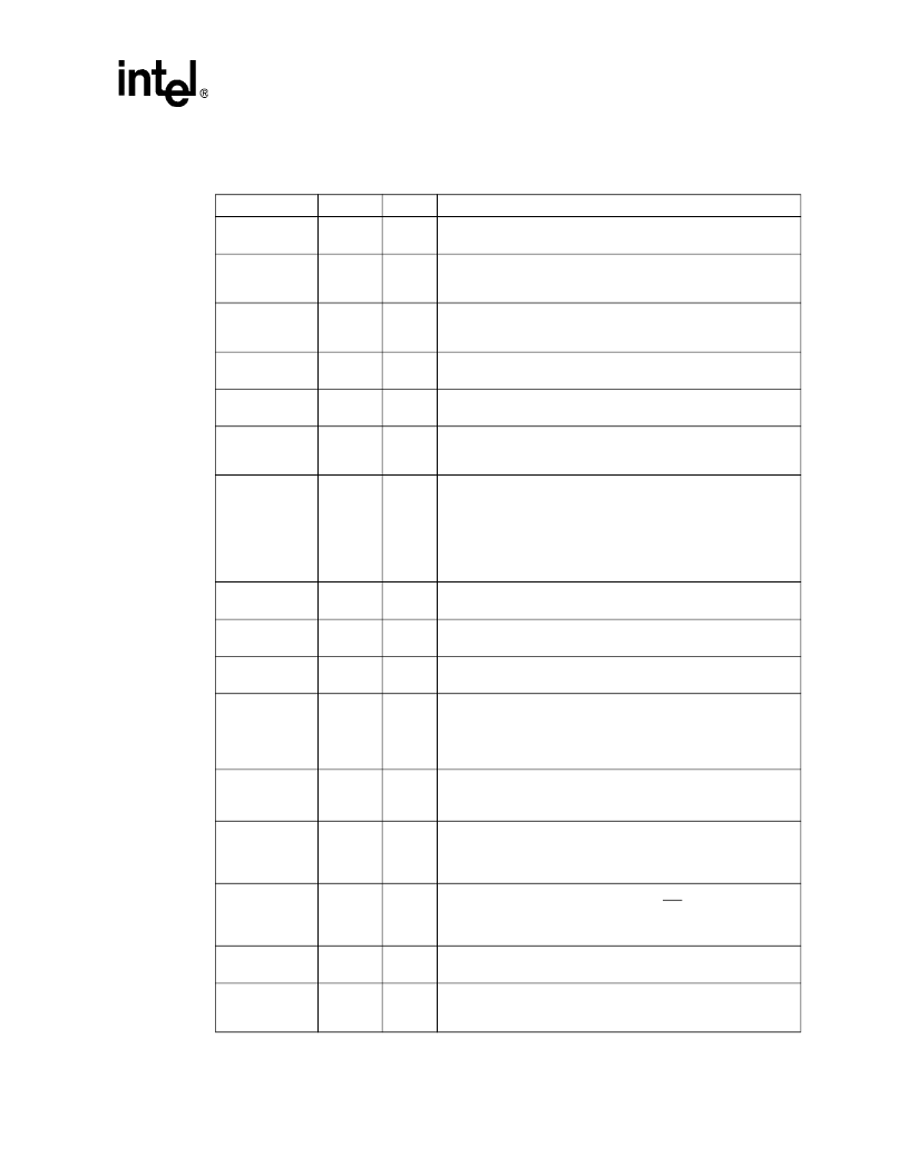
Table 4.
Memory Controller Signals (Sheet 1 of 3)
NAME
COUNT
TYPE
DESCRIPTION
DCLKOUT
1
O
Irst(Q)
SDRAM OUTPUT CLOCK
dedicated for SDRAM memory
subsystem.
DCLKIN
1
I
SDRAM INPUT CLOCK
dedicated for SDRAM memory
subsystem. Used to skew DCLKOUT appropriately to
accommodate flight time and clock buffer delays.
SA[11:0]
12
O
Irst(Q)
SDRAM MULTIPLEXED ADDRESS BUS
carries the multiplexed
row and column addresses to the SDRAM memory banks. For
SA[10]
, see note 1.
SBA[1:0]
2
O
Irst(Q)
SDRAM INTERNAL BANK SELECT
indicates which of the SDRAM
internal banks are read or written during the current transaction.
SRAS#
1
O
Irst(1)
SDRAM ROW ADDRESS STROBE
indicates the presence of a valid
row address on the Multiplexed Address Bus
SA[11:0]
. See note 1.
SCAS#
1
O
Irst(1)
SDRAM COLUMN ADDRESS STROBE
indicates the presence of
a valid column address on the Multiplexed Address Bus
SA[11:0]
.
See note 1.
SDQM[7:0]
8
O
Irst(1)
SDRAM DATA MASK
controls which of the eight bytes on the data
bus should be written or read. When
SDQM[7:0]
asserted, the
SDRAM devices do not accept/drive valid data from/to the byte
lanes. When
SDQM[7:0]
deasserted, the SDRAM devices
accept/drive valid data from/to the byte lanes.
By convention, SDQM[1] masks two x8 SDRAM devices.
Functionally, all
SDQM[7:0]
signals are equivalent.
SWE#
1
O
Irst(1)
SDRAM WRITE ENABLE
indicates that the current memory
transaction is a write operation. See note 1.
SCE[1:0]#
2
O
Irst(1)
SDRAM CHIP ENABLE
enables the SDRAM devices for a
memory access (1 per bank supported). See note 1.
SCKE[1:0]
2
O
Irst(Q)
SCKE[1:0]
are the clock enables for the SDRAM memory.
Deasserting will place the SDRAM in self-refresh mode. See note 1.
DQ[63:0]
64
I/O
Irst(1)
Sync(D)
DATA BUS
carries 64-bit data to and from memory. During a data
(T
d
) cycle, read or write data is present on one or more contiguous
bytes, comprising DQ[63:56], DQ[55:48], DQ[47:40], DQ[39:32],
DQ[31:24], DQ[23:16], DQ[15:8] and DQ[7:0]. During write
operations, unused pins are driven to determinate values.
SCB[7:0]
8
I/O
Irst(1)
Sync(D)
ERROR CORRECTION CODE
carries the 8-bit ECC code to and
from memory during data cycles.
ROE#
1
O
Irst(1)
ROM OUTPUT ENABLE
specifies, during a T
a
cycle, whether the
operation is a write (1) or read (0) to the ROM interface. It remains
valid during T
d
cycles. When
ROE#
is asserted, the data is
transferred from the memory on
RAD[16:9]
.
RWE#
1
O
Irst(1)
ROM WRITE ENABLE
indicates the direction data is to be
transferred to/from ROM and controls the WE input on the ROM
device. When
RWE#
is asserted, the data is transferred to the
memory on DQ[7:0].
RCE[1:0]#
2
O
Irst(1)
FLASH CHIP ENABLE
enables Flash devices for a memory access.
RALE
1
O
Irst(0)
ROM ADDRESS LATCH ENABLE
indicates the cycle in which the
address on RAD[16:3] should be externally latched for the Flash
subsystem.
相關(guān)PDF資料 |
PDF描述 |
|---|---|
| 80960SA | Embedded 32-Bit Microprocessor With 16-Bit Burst Data Bus(帶有16位脈沖串?dāng)?shù)據(jù)總線的嵌入式 32-BIT微處理器) |
| 80960SB | Embedded 32-Bit Microprocessor With 16-Bit Burst Data Bus(帶有16位脈沖串?dāng)?shù)據(jù)總線的嵌入式 32-BIT微處理器) |
| 8097JF | COMMERCIAL/EXPRESS HMOS MICROCONTOLLER |
| 8098 | COMMERCIAL/EXPRESS HMOS MICROCONTROLLER |
| 8098 | T-1 Subminiature Lamps |
相關(guān)代理商/技術(shù)參數(shù) |
參數(shù)描述 |
|---|---|
| 80960SA | 制造商:INTEL 制造商全稱:Intel Corporation 功能描述:EMBEDDED 32-BIT MICROPROCESSOR WITH 16-BIT BURST DATA BUS |
| 80960SB | 制造商:INTEL 制造商全稱:Intel Corporation 功能描述:EMBEDDED 32-BIT MICROPROCESSOR WITH 16-BIT BURST DATA BUS |
| 80961-01 | 制造商:Glenair 功能描述:EARTH BOND M10 FOR AL 4MM T |
| 809621-000 | 制造商:TE Connectivity 功能描述:809621-000 |
| 80963 | 制造商:3M Electronic Products Division 功能描述:Tape Temflex 1500 Brown 15mmx10m |
發(fā)布緊急采購(gòu),3分鐘左右您將得到回復(fù)。