- 您現(xiàn)在的位置:買(mǎi)賣(mài)IC網(wǎng) > PDF目錄378217 > 82845GE (Intel Corp.) 82845GE Graphics and Memory Controller Hub (GMCH) and 82845PE Memory Controller Hub (MCH) PDF資料下載
參數(shù)資料
| 型號(hào): | 82845GE |
| 廠商: | Intel Corp. |
| 英文描述: | 82845GE Graphics and Memory Controller Hub (GMCH) and 82845PE Memory Controller Hub (MCH) |
| 中文描述: | 82845GE圖形和內(nèi)存控制器中樞(GMCH)和82845PE內(nèi)存控制器中樞(MCH) |
| 文件頁(yè)數(shù): | 69/157頁(yè) |
| 文件大小: | 1407K |
| 代理商: | 82845GE |
第1頁(yè)第2頁(yè)第3頁(yè)第4頁(yè)第5頁(yè)第6頁(yè)第7頁(yè)第8頁(yè)第9頁(yè)第10頁(yè)第11頁(yè)第12頁(yè)第13頁(yè)第14頁(yè)第15頁(yè)第16頁(yè)第17頁(yè)第18頁(yè)第19頁(yè)第20頁(yè)第21頁(yè)第22頁(yè)第23頁(yè)第24頁(yè)第25頁(yè)第26頁(yè)第27頁(yè)第28頁(yè)第29頁(yè)第30頁(yè)第31頁(yè)第32頁(yè)第33頁(yè)第34頁(yè)第35頁(yè)第36頁(yè)第37頁(yè)第38頁(yè)第39頁(yè)第40頁(yè)第41頁(yè)第42頁(yè)第43頁(yè)第44頁(yè)第45頁(yè)第46頁(yè)第47頁(yè)第48頁(yè)第49頁(yè)第50頁(yè)第51頁(yè)第52頁(yè)第53頁(yè)第54頁(yè)第55頁(yè)第56頁(yè)第57頁(yè)第58頁(yè)第59頁(yè)第60頁(yè)第61頁(yè)第62頁(yè)第63頁(yè)第64頁(yè)第65頁(yè)第66頁(yè)第67頁(yè)第68頁(yè)當(dāng)前第69頁(yè)第70頁(yè)第71頁(yè)第72頁(yè)第73頁(yè)第74頁(yè)第75頁(yè)第76頁(yè)第77頁(yè)第78頁(yè)第79頁(yè)第80頁(yè)第81頁(yè)第82頁(yè)第83頁(yè)第84頁(yè)第85頁(yè)第86頁(yè)第87頁(yè)第88頁(yè)第89頁(yè)第90頁(yè)第91頁(yè)第92頁(yè)第93頁(yè)第94頁(yè)第95頁(yè)第96頁(yè)第97頁(yè)第98頁(yè)第99頁(yè)第100頁(yè)第101頁(yè)第102頁(yè)第103頁(yè)第104頁(yè)第105頁(yè)第106頁(yè)第107頁(yè)第108頁(yè)第109頁(yè)第110頁(yè)第111頁(yè)第112頁(yè)第113頁(yè)第114頁(yè)第115頁(yè)第116頁(yè)第117頁(yè)第118頁(yè)第119頁(yè)第120頁(yè)第121頁(yè)第122頁(yè)第123頁(yè)第124頁(yè)第125頁(yè)第126頁(yè)第127頁(yè)第128頁(yè)第129頁(yè)第130頁(yè)第131頁(yè)第132頁(yè)第133頁(yè)第134頁(yè)第135頁(yè)第136頁(yè)第137頁(yè)第138頁(yè)第139頁(yè)第140頁(yè)第141頁(yè)第142頁(yè)第143頁(yè)第144頁(yè)第145頁(yè)第146頁(yè)第147頁(yè)第148頁(yè)第149頁(yè)第150頁(yè)第151頁(yè)第152頁(yè)第153頁(yè)第154頁(yè)第155頁(yè)第156頁(yè)第157頁(yè)
Intel
82845MP/82845MZ Chipset-Mobile (MCH-M)
250687-002
Datasheet
69
R
3.7.23.
SMRAM – System Management RAM Control Register – Device
#0
Address Offset:
9Dh
Default Value:
02h
Access:
Read/Write, Read Only, Lock
Size:
8 bits
The SMRAMC register controls how accesses to Compatible and Extended SMRAM spaces are treated.
The Open, Close, and Lock bits function only when G_SMRAME bit is set to a 1. Also, the OPEN bit
must be reset before the LOCK bit is set.
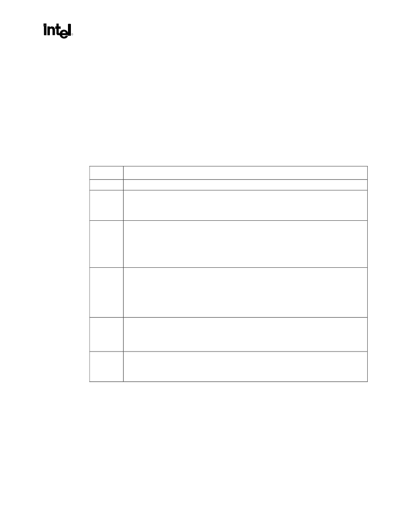
Bit
Description
7
Reserved
6
SMM Space Open (D_OPEN):
When D_OPEN=1 and D_LCK=0, the SMM space DRAM is made
visible even when SMM decode is not active. This is intended to help BIOS initialize SMM space.
Software should ensure that D_OPEN=1 and D_CLS=1 are not set at the same time. When D_LCK
is set to a 1, D_OPEN is reset to 0 and becomes read only.
5
SMM Space Closed (D_CLS):
When D_CLS = 1 SMM space DRAM is not accessible to data
references, even if SMM decode is active. Code references may still access SMM space DRAM. This
will allow SMM software to reference “through” SMM space to update the display even when SMM is
mapped over the VGA range. Software should ensure that D_OPEN=1 and D_CLS=1 are not set at
the same time.
Note that the D_CLS bit only applies to Compatible SMM space.
4
SMM Space Locked (D_LCK):
When D_LCK is set to 1 then D_OPEN is reset to 0 and D_LCK,
D_OPEN, C_BASE_SEG, H_SMRAM_EN, TSEG_SZ and TSEG_EN become “Read Only”. D_LCK
can be set to 1 via a normal configuration space write but can only be cleared by a Full Reset. The
combination of D_LCK and D_OPEN provide convenience with security. The BIOS can use the
D_OPEN function to initialize SMM space and then use D_LCK to “l(fā)ock down” SMM space in the
future so that no application software (or BIOS itself) can violate the integrity of SMM space, even if
the program has knowledge of the D_OPEN function.
3
Global SMRAM Enable (G_SMRAME).
If set to a 1, then Compatible SMRAM functions is enabled,
providing 128 KB of DRAM accessible at the A0000h address while in SMM (ADS# with SMM
decode). To enable Extended SMRAM function this bit has to be set to 1.
Once D_LCK is set, this bit becomes read only.
2:0
Compatible SMM Space Base Segment (C_BASE_SEG) (RO).
This field indicates the location of
SMM space. “SMM DRAM” is not remapped. It is simply “made visible” if the conditions are right to
access SMM space, otherwise the access is forwarded to the hub interface. C_BASE_SEG is
hardwired to 010 to indicate that the MCH-M supports the SMM space at A0000h-BFFFFh.
相關(guān)PDF資料 |
PDF描述 |
|---|---|
| 8284A | Clock Generator and Driver for 8066, 8088 Processors |
| 8284A-1 | Clock Generator and Driver for 8066, 8088 Processors |
| 8284 | TWO-OUTPUT LNB SUPPLY AND CONTROL-VOLTAGE REGULATOR |
| 82865G | Intel 865G/865GV Graphics and Memory Controller Hub |
| 82865GV | Intel 865G/865GV Graphics and Memory Controller Hub |
相關(guān)代理商/技術(shù)參數(shù) |
參數(shù)描述 |
|---|---|
| 82845GL | 制造商:INTEL 制造商全稱(chēng):Intel Corporation 功能描述:Intel 82845G/82845GL/82845GV Graphics and Memory Controller Hub (GMCH) |
| 82845GV | 制造商:INTEL 制造商全稱(chēng):Intel Corporation 功能描述:Intel 82845G/82845GL/82845GV Graphics and Memory Controller Hub (GMCH) |
| 82845GX | 制造商:INTEL 制造商全稱(chēng):Intel Corporation 功能描述:Intel 82845G/82845GL/82845GV Graphics and Memory Controller Hub (GMCH) |
| 82845MP | 制造商:INTEL 制造商全稱(chēng):Intel Corporation 功能描述:Intel 845 Family Chipset-Mobile 82845MP/82845MZ Chipset Memory Controller Hub Mobile (MCH-M) |
| 82845MX | 制造商:INTEL 制造商全稱(chēng):Intel Corporation 功能描述:Intel 845 Family Chipset-Mobile 82845MP/82845MZ Chipset Memory Controller Hub Mobile (MCH-M) |
發(fā)布緊急采購(gòu),3分鐘左右您將得到回復(fù)。