- 您現(xiàn)在的位置:買賣IC網(wǎng) > PDF目錄373891 > AD6634PCB (Analog Devices, Inc.) 80 MSPS, Dual-Channel WCDMA Receive Signal Processor (RSP) PDF資料下載
參數(shù)資料
| 型號: | AD6634PCB |
| 廠商: | Analog Devices, Inc. |
| 元件分類: | 基帶處理器 |
| 英文描述: | 80 MSPS, Dual-Channel WCDMA Receive Signal Processor (RSP) |
| 中文描述: | 80 MSPS的雙通道的WCDMA接收信號處理器(RSP) |
| 文件頁數(shù): | 33/52頁 |
| 文件大小: | 925K |
| 代理商: | AD6634PCB |
第1頁第2頁第3頁第4頁第5頁第6頁第7頁第8頁第9頁第10頁第11頁第12頁第13頁第14頁第15頁第16頁第17頁第18頁第19頁第20頁第21頁第22頁第23頁第24頁第25頁第26頁第27頁第28頁第29頁第30頁第31頁第32頁當前第33頁第34頁第35頁第36頁第37頁第38頁第39頁第40頁第41頁第42頁第43頁第44頁第45頁第46頁第47頁第48頁第49頁第50頁第51頁第52頁
REV. 0
AD6634
–33–
4. Set the Start on Pin Sync bit and the appropriate Sync Pin
Enable high (Ext Address 4 ) (A, B, C, or D).
5. When the Sync pin is sampled high by the AD6634 CLK, this
enables the count down of the Start Update Hold-Off Counter.
The counter is clocked with the AD6634 CLK signal. When it
reaches a count of 1, the Sleep bit of the appropriate channel(s)
is set low to activate the channel(s).
Hop
Hop is a jump from one NCO frequency to a new NCO
frequency. This change in frequency can be synchronized via
microprocessor control (Soft Sync) or an external Sync signal
(PIN Sync) as described below.
To set the NCO frequency without synchronization the following
method should be used.
Set Freq No Hop
1. Set the NCO Freq Hold-Off counter to 0.
2. Load the appropriate NCO frequency. The new frequency
will be immediately loaded to the NCO.
Hop with Soft Sync
The AD6634 includes the ability to synchronize a change in NCO
frequency of multiple channels or chips under microprocessor
control. The NCO Freq Hold-Off counter (0x84) in conjunction
with the Hop bit and the Sync bit (Ext Address 4) allow this
synchronization. Basically the NCO Freq Hold-Off counter
delays the new frequency from being loaded into the NCO by
its value (number of AD6634 CLKs). The following method is
used to synchronize a hop in frequency of multiple channels via
microprocessor control.
1. Note that the time from when DTACK (Pin 57) goes high to
when the NCO begins processing data is the contents of the
NCO Freq Hold-Off counter (0x84) + 7 master clock cycles.
2. Write the NCO Freq Hold-Off (0x84) counter to the appro-
priate value (greater than 1 and less then 2
16
–1).
3. Write the NCO Frequency register(s) to the new desired
frequency.
4. Write the Hop bit and the Sync(s) bit high (Ext Address 4).
5. This starts the NCO Freq Hold-Off counter counting down.
The counter is clocked with the AD6634 CLK signal. When
it reaches a count of 1, the new frequency is loaded into
the NCO.
Hop with Pin Sync
The AD6634 include four Sync pins to provide the most accu-
rate synchronization, especially between multiple AD6634s.
Synchronization of hopping to a new NCO frequency with an
external signal is accomplished with the following method.
1. Note that the time from when the SYNC pin goes high to
when the NCO begins processing data is the contents of the
NCO Freq Hold-Off counter (0x84) + 5 master clock cycles.
2. Write the NCO Freq Hold-Off counter(s) (0x84) to the
appropriate value (greater than 1 and less than 2
16
–1).
3. Write the NCO Frequency register(s) to the new desired
frequency.
4. Set the Hop on Pin Sync bit and the appropriate Sync Pin
Enable high.
5. When the selected Sync pin is sampled high by the AD6634
CLK, this enables the countdown of the NCO Freq Hold-Off
counter. The counter is clocked with the AD6634 CLK signal.
When it reaches a count of 1, the new frequency is loaded
into the NCO.
PARALLEL OUTPUT PORTS
The AD6634 incorporates two independent 16-bit parallel ports
for output data transfer. Both parallel ports share pins and internal
mux circuitry. A single parallel port and a single Link Port can
be used simultaneously, but only if they do not share the same
data path; the two possible choices are Parallel Port A with
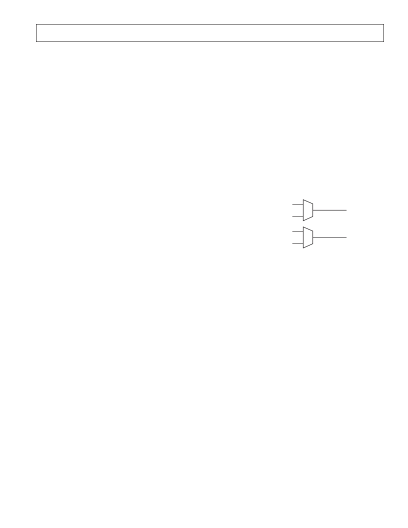
Link Port B, or Parallel Port B with Link Port A. Figure 35
presents a simplified block diagram showing the AD6634’s output
data routing configuration.
OUTPUT PORT A
PARALLEL PORT A
LINK PORT A
OUTPUT PORT B
PARALLEL PORT B
LINK PORT B
Figure 35. Output Port Data Routing
Parallel port configuration is specified by accessing Port Control
Register addresses 0x1A and 0x1C for parallel ports A and B,
respectively. Port clock Master/Slave mode (described later) is
configured using the Port Clock Control register at address
0x1E. Note that to access these registers, Bit 5 (Access Port
Control Registers) of external address 3 (SLEEP register) must
be set. The address is then selected by programming the CAR
register at external address 6.
The parallel ports are enabled by setting Bit 7 of the Link Control
registers at addresses 0x1B and 0x1D for ports A and B,
respectively.
Each parallel port is capable of operating in either Channel mode
or AGC mode. Each mode is described in detail below.
Channel Mode
Parallel port Channel mode is selected by setting Bit 0 of addresses
0x1B and 0x1D for parallel ports A and B, respectively. In
Channel mode, I and Q words from each channel is directed to
the parallel port, bypassing the AGC. The specific channels
output by the port are selected by setting Bits 1 through 4 of
Parallel Port Control Register 0x1A (port A) and 0x1C (port B).
Channel mode provides two data formats. Each format requires a
different number of parallel port clock (PCLK) cycles to complete
the transfer of data. In each case, each data element is trans-
ferred during one PCLK cycle. See Figures 36 and 37, which
present Channel mode parallel port timing.
相關PDF資料 |
PDF描述 |
|---|---|
| AD6635 | 4-Channel, 80 MSPS WCDMA Receive Signal Processor (RSP) |
| AD6635BB | 4-Channel, 80 MSPS WCDMA Receive Signal Processor (RSP) |
| AD6636 | 150 MSPS Wideband Digital Down-Converter (DDC) |
| AD6636BBCZ1 | 150 MSPS Wideband Digital Down-Converter (DDC) |
| AD6636BC | 150 MSPS Wideband Digital Down-Converter (DDC) |
相關代理商/技術參數(shù) |
參數(shù)描述 |
|---|---|
| AD6635 | 制造商:AD 制造商全稱:Analog Devices 功能描述:4-Channel, 80 MSPS WCDMA Receive Signal Processor (RSP) |
| AD6635BB | 功能描述:IC RSP 80MSPS QUAD 324-BGA RoHS:否 類別:RF/IF 和 RFID >> RF 混頻器 系列:AD6635 產(chǎn)品培訓模塊:Lead (SnPb) Finish for COTS Obsolescence Mitigation Program 標準包裝:100 系列:- RF 型:W-CDMA 頻率:2.11GHz ~ 2.17GHz 混頻器數(shù)目:1 增益:17dB 噪音數(shù)據(jù):2.2dB 次要屬性:- 電流 - 電源:11.7mA 電源電壓:2.7 V ~ 3.3 V 包裝:托盤 封裝/外殼:12-VFQFN 裸露焊盤 供應商設備封裝:12-QFN-EP(3x3) |
| AD6635BB/PCB | 制造商:Analog Devices 功能描述:Evaluation Kit For 4-Channel, 80MSPS WCDMA Receive Signal Processor |
| AD6635BBZ | 制造商:Analog Devices 功能描述:Receive Signal Processor 324-Pin BGA |
| AD6636 | 制造商:AD 制造商全稱:Analog Devices 功能描述:150 MSPS Wideband Digital Down-Converter (DDC) |
發(fā)布緊急采購,3分鐘左右您將得到回復。