- 您現(xiàn)在的位置:買賣IC網(wǎng) > PDF目錄373891 > AD6653 (Analog Devices, Inc.) IF Diversity Receiver PDF資料下載
參數(shù)資料
| 型號: | AD6653 |
| 廠商: | Analog Devices, Inc. |
| 英文描述: | IF Diversity Receiver |
| 中文描述: | IF分集接收機(jī) |
| 文件頁數(shù): | 16/80頁 |
| 文件大小: | 1998K |
| 代理商: | AD6653 |
第1頁第2頁第3頁第4頁第5頁第6頁第7頁第8頁第9頁第10頁第11頁第12頁第13頁第14頁第15頁當(dāng)前第16頁第17頁第18頁第19頁第20頁第21頁第22頁第23頁第24頁第25頁第26頁第27頁第28頁第29頁第30頁第31頁第32頁第33頁第34頁第35頁第36頁第37頁第38頁第39頁第40頁第41頁第42頁第43頁第44頁第45頁第46頁第47頁第48頁第49頁第50頁第51頁第52頁第53頁第54頁第55頁第56頁第57頁第58頁第59頁第60頁第61頁第62頁第63頁第64頁第65頁第66頁第67頁第68頁第69頁第70頁第71頁第72頁第73頁第74頁第75頁第76頁第77頁第78頁第79頁第80頁
AD6653
Rev. 0 | Page 16 of 80
0
PIN 1
INDICATOR
1
D
1
D
1
D
2
D
2
D
2
D
2
D
2
D
2
D
2
D
2
D
2
D
2
D
3
D
3
D
3
D
6
6
6
6
6
5
5
5
5
5
5
5
5
5
5
4
D
D
D
F
F
F
F
D
F
F
F
F
S
C
C
C
1
2
3
4
5
6
7
8
9
10
11
12
13
14
15
16
DRVDD
DNC
DNC
D0– (LSB)
D0+ (LSB)
D1–
D1+
D2–
D2+
DCO–
DCO+
D3–
D3+
D4–
D4+
D5–
DNC = DO NOT CONNECT
SCLK/DFS
SDIO/DCS
AVDD
AVDD
VIN+B
VIN–B
RBIAS
CML
SENSE
VREF
VIN–A
VIN+A
AVDD
SMI SDFS
SMI SCLK/PDWN
SMI SDO/OEB
48
47
46
45
44
43
42
41
40
39
38
37
36
35
34
33
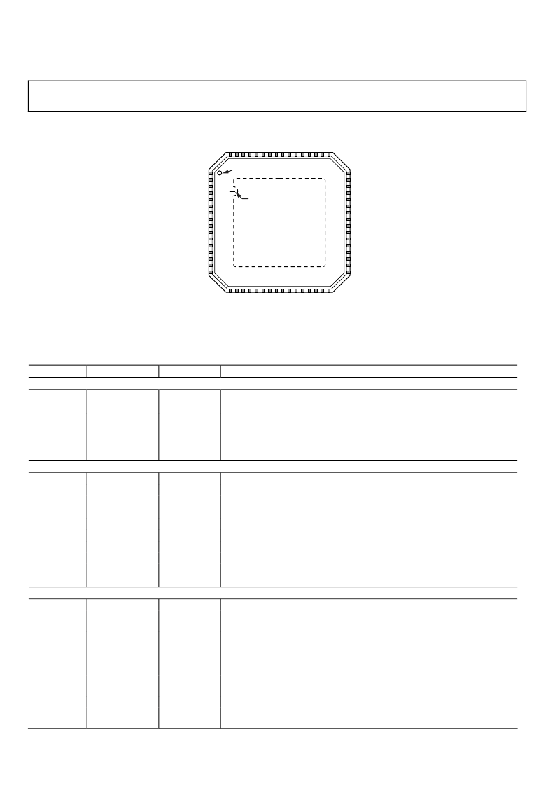
AD6653
PARALLEL LVDS
TOP VIEW
(Not to Scale)
EXPOSED PADDLE, PIN 0
(BOTTOM OF PACKAGE)
Figure 10. LFCSP Interleaved Parallel LVDS Pin Configuration (Top View)
Table 9. Pin Function Descriptions (Interleaved Parallel LVDS Mode)
Pin No.
Mnemonic
ADC Power Supplies
20, 64
DRGND
1, 21
DRVDD
24, 57
DVDD
36, 45, 46
AVDD
0
AGND
2, 3, 62, 63
DNC
ADC Analog
37
VIN+A
38
VINA
44
VIN+B
43
VINB
39
VREF
40
SENSE
42
RBIAS
41
CML
49
CLK+
50
CLK
ADC Fast Detect Outputs
54
FD0+
53
FD0
Type
Description
Ground
Supply
Supply
Supply
Ground
Digital Output Ground.
Digital Output Driver Supply (1.8 V to 3.3 V).
Digital Power Supply (1.8 V Nominal).
Analog Power Supply (1.8 V Nominal).
Analog Ground. Pin 0 is the exposed thermal pad on the bottom of the package.
Do Not Connect.
Input
Input
Input
Input
Input/Output
Input
Input/Output
Output
Input
Input
Differential Analog Input Pin (+) for Channel A.
Differential Analog Input Pin () for Channel A.
Differential Analog Input Pin (+) for Channel B.
Differential Analog Input Pin () for Channel B.
Voltage Reference Input/Output.
Voltage Reference Mode Select. See Table 11 for details.
External Reference Bias Resistor.
Common-Mode Level Bias Output for Analog Inputs.
ADC Clock Input—True.
ADC Clock Input—Complement.
Output
Output
Channel A/Channel B LVDS Fast Detect Indicator 0—True. See Table 17 for details.
Channel A/Channel B LVDS Fast Detect Indicator 0—Complement. See Table 17
for details.
Channel A/Channel B LVDS Fast Detect Indicator 1—True. See Table 17 for details.
Channel A/Channel B LVDS Fast Detect Indicator 1—Complement. See Table 17
for details.
Channel A/Channel B LVDS Fast Detect Indicator 2—True. See Table 17 for details.
Channel A/Channel B LVDS Fast Detect Indicator 2—Complement. See Table 17
for details.
Channel A/Channel B LVDS Fast Detect Indicator 3—True. See Table 17 for details.
Channel A/Channel B LVDS Fast Detect Indicator 3—Complement. See Table 17
for details.
56
55
FD1+
FD1
Output
Output
59
58
FD2+
FD2
Output
Output
61
60
FD3+
FD3
Output
Output
相關(guān)PDF資料 |
PDF描述 |
|---|---|
| AD6653-125EBZ | IF Diversity Receiver |
| AD6653BCPZ-125 | IF Diversity Receiver |
| AD6653BCPZ-150 | IF Diversity Receiver |
| AD6655BCPZ-1251 | IF Diversity Receiver |
| AD6655 | IF Diversity Receiver |
相關(guān)代理商/技術(shù)參數(shù) |
參數(shù)描述 |
|---|---|
| AD6653-125EBZ | 制造商:Analog Devices 功能描述:Evaluation Board For AD6653 制造商:Analog Devices 功能描述:EVAL BD FOR AD6653 - Bulk 制造商:Analog Devices 功能描述:KIT EVALUATION BOARD AD6653 |
| AD6653-150EBZ | 制造商:Analog Devices 功能描述:EVAL BD FOR AD6653 - Bulk |
| AD6653BCPZ-125 | 制造商:Analog Devices 功能描述:IF DIVERSITY RCVR 64LFCSP EP - Trays 制造商:Rochester Electronics LLC 功能描述: 制造商:Analog Devices 功能描述:IC RECEIVER IF DIVERSITY LFCSP64 |
| AD6653BCPZ-150 | 制造商:Analog Devices 功能描述:IF DIVERSITY RCVR 64LFCSP EP - Trays 制造商:Analog Devices 功能描述:IC RECEIVER IF DIVERSITY LFCSP64 制造商:Analog Devices 功能描述:IC, RECEIVER, IF DIVERSITY, LFCSP64 |
| AD6654 | 制造商:Analog Devices 功能描述:- Bulk |
發(fā)布緊急采購,3分鐘左右您將得到回復(fù)。