- 您現(xiàn)在的位置:買賣IC網(wǎng) > PDF目錄378286 > ADE7763ARS (ANALOG DEVICES INC) Single-Phase Active and Apparent Energy Metering IC PDF資料下載
參數(shù)資料
| 型號(hào): | ADE7763ARS |
| 廠商: | ANALOG DEVICES INC |
| 元件分類: | 電源管理 |
| 英文描述: | Single-Phase Active and Apparent Energy Metering IC |
| 中文描述: | 2-CHANNEL POWER SUPPLY SUPPORT CKT, PDSO20 |
| 封裝: | MO-150AE, SSOP-20 |
| 文件頁(yè)數(shù): | 44/56頁(yè) |
| 文件大?。?/td> | 1328K |
| 代理商: | ADE7763ARS |
第1頁(yè)第2頁(yè)第3頁(yè)第4頁(yè)第5頁(yè)第6頁(yè)第7頁(yè)第8頁(yè)第9頁(yè)第10頁(yè)第11頁(yè)第12頁(yè)第13頁(yè)第14頁(yè)第15頁(yè)第16頁(yè)第17頁(yè)第18頁(yè)第19頁(yè)第20頁(yè)第21頁(yè)第22頁(yè)第23頁(yè)第24頁(yè)第25頁(yè)第26頁(yè)第27頁(yè)第28頁(yè)第29頁(yè)第30頁(yè)第31頁(yè)第32頁(yè)第33頁(yè)第34頁(yè)第35頁(yè)第36頁(yè)第37頁(yè)第38頁(yè)第39頁(yè)第40頁(yè)第41頁(yè)第42頁(yè)第43頁(yè)當(dāng)前第44頁(yè)第45頁(yè)第46頁(yè)第47頁(yè)第48頁(yè)第49頁(yè)第50頁(yè)第51頁(yè)第52頁(yè)第53頁(yè)第54頁(yè)第55頁(yè)第56頁(yè)
ADE7763
SUSPENDING FUNCTIONALITY
The analog and the digital circuit can be suspended separately.
The analog portion can be suspended by setting the ASUSPEND
bit (Bit 4) of the mode register to logic high—see the Mode
Register (0x09) section. In suspend mode, all waveform samples
from the ADCs are set to 0s. The digital circuitry can be halted
by stopping the CLKIN input and maintaining a logic high or
low on the CLKIN pin. The ADE7763 can be reactivated by
restoring the CLKIN input and setting the ASUSPEND bit to
logic low.
Rev. A | Page 44 of 56
CHECKSUM REGISTER
The ADE7763 has a checksum register (CHECKSUM[5:0]) to
ensure that the data bits received in the last serial read operation
are not corrupted. The 6-bit checksum register is reset before
the first bit (MSB of the register to be read) is put on the DOUT
pin. During a serial read operation, when each data bit becomes
available upon the rising edge of SCLK, the bit is added to the
checksum register. At the end of the serial read operation, the
content of the checksum register is equal to the sum of all ones
previously read in the register. Using the checksum register, the
user can determine if an error has occurred during the last read
operation. Note that a read to the checksum register also
generates a checksum of the checksum register itself.
CONTENT OF REGISTER (n-bytes)
CHECKSUM REGISTER
ADDR: 0x3E
+
+
DOUT
0
Figure 79. Checksum Register for Serial Interface Read
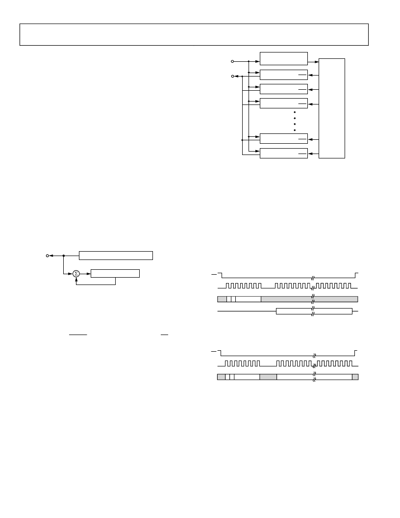
SERIAL INTERFACE
All ADE7763 functionality is accessible via several on-chip
registers—see Figure 80. The contents of these registers can be
updated or read using the on-chip serial interface. After power-
on or toggling the RESET pin low and a falling edge on CS, the
ADE7763 is placed in communication mode. In co
tion mode, the ADE7763 expects a write to its communication
to the communication register
register. The data written
determines whether the next data transfer operation is a read or
a write and which register is accessed. Therefore, all data
transfer operations with the ADE7763, whether a read or a
write, must begin with a write to the communication register.
mmunica-
COMMUNICATION
REGISTER
IN
OUT
IN
OUT
IN
OUT
IN
OUT
IN
OUT
REGISTER 1
REGISTER 2
REGISTER 3
REGISTER n–1
REGISTER n
REGISTER
ADDRESS
DECODE
DIN
DOUT
0
Figure 80. Addressing ADE7763 Registers via the Communication Register
The communication register is an 8-bit-wide register. The MSB
determines whether the next data transfer operation is a read or
a write. The 6 LSBs contain the address of the register to be
accessed—see the Communication Register section for a more
detailed description.
Figure 81 and Figure 82 show the data transfer sequences for a
read and write operation, respectively. Upon completion of a
data transfer (read or write), the ADE7763 again enters the
communication mode. A data transfer is complete when the
LSB of the ADE7763 register being addressed (for a write or a
read) is transferred to or from the ADE7763.
MULTIBYTE
COMMUNICATION REGISTER WRITE
ADDRESS
0
0
DIN
SCLK
CS
DOUT
READ DATA
0
Figure 81. Reading Data from the ADE7763 via the Serial Interface
COMMUNICATION REGISTER WRITE
ADDRESS
0
1
DIN
SCLK
CS
0
0
A
MULTIBYTE
READ DATA
Figure 82. Writing Data to the ADE7763 via the Serial Interface
相關(guān)PDF資料 |
PDF描述 |
|---|---|
| ADE7763ARSRL | Single-Phase Active and Apparent Energy Metering IC |
| ADG804 | 0.5 ohm CMOS 1.65 V TO 3.6 V 4-Channel Multiplexer |
| ADG804YRM | 0.5 ohm CMOS 1.65 V TO 3.6 V 4-Channel Multiplexer |
| ADG804YRM-REEL | 0.5 ohm CMOS 1.65 V TO 3.6 V 4-Channel Multiplexer |
| ADG804YRM-REEL7 | 0.5 ohm CMOS 1.65 V TO 3.6 V 4-Channel Multiplexer |
相關(guān)代理商/技術(shù)參數(shù) |
參數(shù)描述 |
|---|---|
| ADE7763ARSRL | 制造商:Analog Devices 功能描述:Energy Measurement 20-Pin SSOP T/R |
| ADE7763ARSZ | 功能描述:IC ENERGY METERING 1PHASE 20SSOP RoHS:是 類別:集成電路 (IC) >> PMIC - 能量測(cè)量 系列:- 產(chǎn)品培訓(xùn)模塊:Lead (SnPb) Finish for COTS Obsolescence Mitigation Program 標(biāo)準(zhǔn)包裝:2,500 系列:* |
| ADE7763ARSZ | 制造商:Analog Devices 功能描述:IC, SINGLE PHASE ENERGY METER, SSOP-20 |
| ADE7763ARSZRL | 功能描述:IC ENERGY METERING 1PHASE 20SSOP RoHS:是 類別:集成電路 (IC) >> PMIC - 能量測(cè)量 系列:- 產(chǎn)品培訓(xùn)模塊:Lead (SnPb) Finish for COTS Obsolescence Mitigation Program 標(biāo)準(zhǔn)包裝:2,500 系列:* |
| ADE7763ARSZRL | 制造商:Analog Devices 功能描述:IC, SINGLE PHASE ENERGY METER, SSOP-20 |
發(fā)布緊急采購(gòu),3分鐘左右您將得到回復(fù)。