- 您現(xiàn)在的位置:買賣IC網(wǎng) > PDF目錄378286 > ADE7763ARSRL (ANALOG DEVICES INC) Single-Phase Active and Apparent Energy Metering IC PDF資料下載
參數(shù)資料
| 型號(hào): | ADE7763ARSRL |
| 廠商: | ANALOG DEVICES INC |
| 元件分類: | 電源管理 |
| 英文描述: | Single-Phase Active and Apparent Energy Metering IC |
| 中文描述: | 2-CHANNEL POWER SUPPLY SUPPORT CKT, PDSO20 |
| 封裝: | MO-150AE, SSOP-20 |
| 文件頁(yè)數(shù): | 8/56頁(yè) |
| 文件大小: | 1328K |
| 代理商: | ADE7763ARSRL |
第1頁(yè)第2頁(yè)第3頁(yè)第4頁(yè)第5頁(yè)第6頁(yè)第7頁(yè)當(dāng)前第8頁(yè)第9頁(yè)第10頁(yè)第11頁(yè)第12頁(yè)第13頁(yè)第14頁(yè)第15頁(yè)第16頁(yè)第17頁(yè)第18頁(yè)第19頁(yè)第20頁(yè)第21頁(yè)第22頁(yè)第23頁(yè)第24頁(yè)第25頁(yè)第26頁(yè)第27頁(yè)第28頁(yè)第29頁(yè)第30頁(yè)第31頁(yè)第32頁(yè)第33頁(yè)第34頁(yè)第35頁(yè)第36頁(yè)第37頁(yè)第38頁(yè)第39頁(yè)第40頁(yè)第41頁(yè)第42頁(yè)第43頁(yè)第44頁(yè)第45頁(yè)第46頁(yè)第47頁(yè)第48頁(yè)第49頁(yè)第50頁(yè)第51頁(yè)第52頁(yè)第53頁(yè)第54頁(yè)第55頁(yè)第56頁(yè)
ADE7763
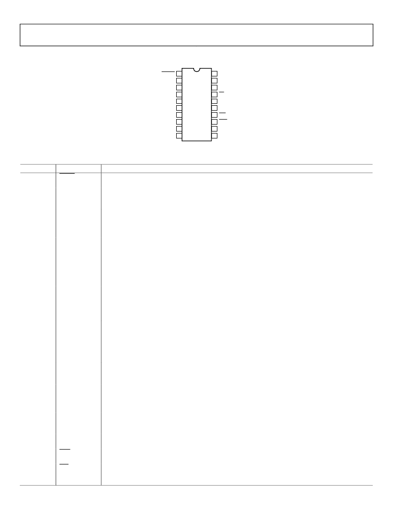
PIN CONFIGURATION AND FUNCTION DESCRIPTIONS
Rev. A | Page 8 of 56
V2N
6
V2P
7
AGND
8
REF
IN/OUT
DGND
10
9
CLKIN
IRQ
SAG
ZX
CF
15
14
13
12
11
ADE7763
TOP VIEW
(Not to Scale)
DVDD
2
AVDD
3
V1P
4
V1N
5
DOUT
SCLK
CS
CLKOUT
19
18
RESET
1
DIN
20
17
16
0
Figure 5. Pin Configuration (SSOP Package)
Table 4. Pin Function Descriptions
Pin No.
Mnemonic
1
RESET
Description
Reset Pin for the ADE7763. A logic low on this pin holds the ADCs and digital circuitry (including the serial
interface) in a reset condition.
Digital Power Supply. This pin provides the supply voltage for the digital circuitry. The supply voltage
should be maintained at 5 V ± 5% for specified operation. This pin should be decoupled to DGND with a
10 μF capacitor in parallel with a ceramic 100 nF capacitor.
Analog Power Supply. This pin provides the supply voltage for the analog circuitry. The supply should be
maintained at 5 V ± 5% for specified operation. Minimize power supply ripple and noise at this pin by using
proper decoupling. The typical performance graphs show the power supply rejection performance. This
pin should be decoupled to AGND with a 10 μF capacitor in parallel with a ceramic 100 nF capacitor.
Analog Inputs for Channel 1. This channel is intended for use with a di/dt current transducer, i.e., a
Rogowski coil or another current sensor such as a shunt or current transformer (CT). These inputs are fully
differential voltage inputs with maximum differential input signal levels of ±0.5 V, ±0.25 V, and ±0.125 V,
depending on the full-scale selection—see the Analog Inputs section. Channel 1 also has a PGA with gain
selections of 1, 2, 4, 8, or 16. The maximum signal level at these pins with respect to AGND is ±0.5 V. Both
inputs have internal ESD protection circuitry and can sustain an overvoltage of ±6 V without risk of
permanent damage.
Analog Inputs for Channel 2. This channel is intended for use with the voltage transducer. These inputs are
fully differential voltage inputs with a maximum differential signal level of ±0.5 V. Channel 2 also has a PGA
with gain selections of 1, 2, 4, 8, or 16. The maximum signal level at these pins with respect to AGND is
±0.5 V. Both inputs have internal ESD protection circuitry and can sustain an overvoltage of ±6 V without
risk of permanent damage.
Analog Ground Reference. This pin provides the ground reference for the analog circuitry, i.e., ADCs and
reference. This pin should be tied to the analog ground plane or to the quietest ground reference in the
system. Use this quiet ground reference for all analog circuitry, such as antialiasing filters and current and
voltage transducers. To minimize ground noise around the ADE7763, connect the quiet ground plane
to the digital ground plane at only one point. It is acceptable to place the entire device on the analog
ground plane.
Access to the On-Chip Voltage Reference. The on-chip reference has a nominal value of 2.4 V ± 8% and a
typical temperature coefficient of 30 ppm/°C. An external reference source can also be connected at this
pin. In either case, this pin should be decoupled to AGND with a 1 μF ceramic capacitor.
Digital Ground Reference. This pin provides the ground reference for the digital circuitry, i.e., multiplier,
filters, and digital-to-frequency converter. Because the digital return currents in the ADE7763 are small, it is
acceptable to connect this pin to the analog ground plane of the system. However, high bus capacitance
on the DOUT pin could result in noisy digital current, which could affect performance.
Calibration Frequency Logic Output. The CF logic output gives active power information. This output is
intended to be used for operational and calibration purposes. The full-scale output frequency can be
adjusted by writing to the CFDEN and CFNUM registers—see the Energy-to-Frequency Conversion section.
Voltage Waveform (Channel 2) Zero-Crossing Output. This output toggles logic high and logic low at the
zero crossing of the differential signal on Channel 2—see the Zero-Crossing Detection section.
This open-drain logic output goes active low when either no zero crossings are detected or a low voltage
threshold (Channel 2) is crossed for a specified duration—see the Line Voltage Sag Detection section.
Interrupt Request Output. This is an active low, open-drain logic output. Maskable interrupts include active
energy register rollover, active energy register at half level, and arrivals of new waveform samples—see the
Interrupts section.
2
DVDD
3
AVDD
4, 5
V1P, V1N
6, 7
V2N, V2P
8
AGND
9
REF
IN/OUT
10
DGND
11
CF
12
ZX
13
SAG
14
IRQ
相關(guān)PDF資料 |
PDF描述 |
|---|---|
| ADG804 | 0.5 ohm CMOS 1.65 V TO 3.6 V 4-Channel Multiplexer |
| ADG804YRM | 0.5 ohm CMOS 1.65 V TO 3.6 V 4-Channel Multiplexer |
| ADG804YRM-REEL | 0.5 ohm CMOS 1.65 V TO 3.6 V 4-Channel Multiplexer |
| ADG804YRM-REEL7 | 0.5 ohm CMOS 1.65 V TO 3.6 V 4-Channel Multiplexer |
| ADN2525 | 10.7 Gbps Active Back-Termination, Differential Laser Diode Driver |
相關(guān)代理商/技術(shù)參數(shù) |
參數(shù)描述 |
|---|---|
| ADE7763ARSZ | 功能描述:IC ENERGY METERING 1PHASE 20SSOP RoHS:是 類別:集成電路 (IC) >> PMIC - 能量測(cè)量 系列:- 產(chǎn)品培訓(xùn)模塊:Lead (SnPb) Finish for COTS Obsolescence Mitigation Program 標(biāo)準(zhǔn)包裝:2,500 系列:* |
| ADE7763ARSZ | 制造商:Analog Devices 功能描述:IC, SINGLE PHASE ENERGY METER, SSOP-20 |
| ADE7763ARSZRL | 功能描述:IC ENERGY METERING 1PHASE 20SSOP RoHS:是 類別:集成電路 (IC) >> PMIC - 能量測(cè)量 系列:- 產(chǎn)品培訓(xùn)模塊:Lead (SnPb) Finish for COTS Obsolescence Mitigation Program 標(biāo)準(zhǔn)包裝:2,500 系列:* |
| ADE7763ARSZRL | 制造商:Analog Devices 功能描述:IC, SINGLE PHASE ENERGY METER, SSOP-20 |
| ADE7768 | 制造商:AD 制造商全稱:Analog Devices 功能描述:Energy Metering IC with Integrated Oscillator and Positive Power Accumulation |
發(fā)布緊急采購(gòu),3分鐘左右您將得到回復(fù)。