- 您現(xiàn)在的位置:買賣IC網(wǎng) > PDF目錄378286 > ADV7183A (Analog Devices, Inc.) Multiformat SDTV Video Decoder PDF資料下載
參數(shù)資料
| 型號(hào): | ADV7183A |
| 廠商: | Analog Devices, Inc. |
| 英文描述: | Multiformat SDTV Video Decoder |
| 中文描述: | 標(biāo)清多格式視頻解碼器 |
| 文件頁(yè)數(shù): | 64/104頁(yè) |
| 文件大小: | 894K |
| 代理商: | ADV7183A |
第1頁(yè)第2頁(yè)第3頁(yè)第4頁(yè)第5頁(yè)第6頁(yè)第7頁(yè)第8頁(yè)第9頁(yè)第10頁(yè)第11頁(yè)第12頁(yè)第13頁(yè)第14頁(yè)第15頁(yè)第16頁(yè)第17頁(yè)第18頁(yè)第19頁(yè)第20頁(yè)第21頁(yè)第22頁(yè)第23頁(yè)第24頁(yè)第25頁(yè)第26頁(yè)第27頁(yè)第28頁(yè)第29頁(yè)第30頁(yè)第31頁(yè)第32頁(yè)第33頁(yè)第34頁(yè)第35頁(yè)第36頁(yè)第37頁(yè)第38頁(yè)第39頁(yè)第40頁(yè)第41頁(yè)第42頁(yè)第43頁(yè)第44頁(yè)第45頁(yè)第46頁(yè)第47頁(yè)第48頁(yè)第49頁(yè)第50頁(yè)第51頁(yè)第52頁(yè)第53頁(yè)第54頁(yè)第55頁(yè)第56頁(yè)第57頁(yè)第58頁(yè)第59頁(yè)第60頁(yè)第61頁(yè)第62頁(yè)第63頁(yè)當(dāng)前第64頁(yè)第65頁(yè)第66頁(yè)第67頁(yè)第68頁(yè)第69頁(yè)第70頁(yè)第71頁(yè)第72頁(yè)第73頁(yè)第74頁(yè)第75頁(yè)第76頁(yè)第77頁(yè)第78頁(yè)第79頁(yè)第80頁(yè)第81頁(yè)第82頁(yè)第83頁(yè)第84頁(yè)第85頁(yè)第86頁(yè)第87頁(yè)第88頁(yè)第89頁(yè)第90頁(yè)第91頁(yè)第92頁(yè)第93頁(yè)第94頁(yè)第95頁(yè)第96頁(yè)第97頁(yè)第98頁(yè)第99頁(yè)第100頁(yè)第101頁(yè)第102頁(yè)第103頁(yè)第104頁(yè)
ADV7183A
MPU PORT DESCRIPTION
The ADV7183A supports a 2-wire (I
2
C compatible) serial inter-
face. Four inputs, serial data (SDA1 and SDA2) and serial clock
(SCLK1 and SCLK2), carry information between the
ADV7183A and the system I
2
C master controller. Each slave
device is recognized by a unique address. The ADV7183A has
two ports: the control port, which allows the user to set up and
configure the decoder; and the VBI data readback port, which
allows the user to read back captured VBI data. Both the control
and VBI ports have four possible slave addresses for both read
and write operations, depending on the logic level on the ALSB
pin. These four unique addresses are shown in Table 170. The
ADV7183A’s ALSB pin controls Bit 1 of the slave address. By
altering the ALSB, it is possible to control two ADV7183As in
an application without having a conflict with the same slave
address. The LSB (Bit 0) sets either a read or write operation.
Logic 1 corresponds to a read operation; Logic 0 corresponds to
a write operation.
Table 170. I
2
C Address for ADV7183A
Slave Address
Control Port
0
0
0x40
0
1
0x41
1
0
0x42
1
1
0x43
Rev. A | Page 64 of 104
ALSB
R/W
Slave Address
VBI Port
0x20
0x21
0x22
0x23
To control the device on the bus, a specific protocol must be
followed. First, the master initiates a data transfer by establish-
ing a Start condition, which is defined by a high-to-low
transition on SDA1/SDA2 while SCLK1/SCLK2 remains high.
This indicates that an address/data stream will follow. All per-
ipherals respond to the Start condition and shift the next eight
bits (7-bit address + R/W bit). The bits are transferred from
MSB down to LSB. The peripheral that recognizes the trans-
mitted address responds by pulling the data line low during the
ninth clock pulse; this is known as an acknowledge bit. All other
devices withdraw from the bus at this point and maintain an
idle condition. The idle condition is where the device monitors
the SDA1/SDA2 and SCLK1/SCLK2 lines, waiting for the Start
condition and the correct transmitted address. The R/W bit
determines the direction of the data. Logic 0 on the LSB of the
first byte means the master will write information to the
peripheral. Logic 1 on the LSB of the first byte means the master
will read information from the peripheral.
The ADV7183A acts as a standard slave device on the bus. The
data on the SDA pin is eight bits long, supporting the 7-bit
addresses plus the R/W bit. The ADV7183A has 196 subad-
dresses to enable access to the internal registers. It therefore
interprets the first byte as the device address and the second
byte as the starting subaddress. The subaddresses auto-
increment, allowing data to be written to or read from the
starting subaddress. A data transfer is always terminated by a
Stop condition. The user can also access any unique subaddress
register on a one-by-one basis without updating all the registers.
Stop and Start conditions can be detected at any stage during
the data transfer. If these conditions are asserted out of
sequence with normal read and write operations, they cause an
immediate jump to the idle condition. During a given SCLK
high period, the user should only issue one Start condition, one
Stop condition, or a single Stop condition followed by a single
Start condition. If an invalid subaddress is issued by the user,
the ADV7183A will not issue an acknowledge and will return to
the idle condition.
If in auto-increment mode the user exceeds the highest
subaddress, the following action is taken:
1.
In read mode, the highest subaddress register contents
continue to be output until the master device issues a no-
acknowledge. This indicates the end of a read. A no-
acknowledge condition is where the SDA line is not pulled
low on the ninth pulse.
2.
In write mode, the data for the invalid byte is not loaded
into any subaddress register, a no acknowledge is issued by
the ADV7183A, and the part returns to the idle condition.
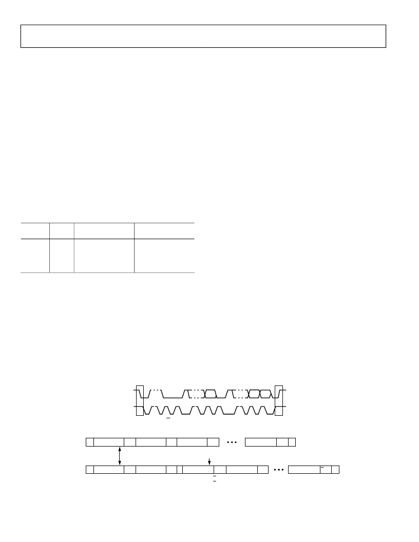
0
SDATA
SCLOCK
START ADDR
ACK
ACK
DATA
ACK
STOP
SUBADDRESS
1–7
1–7
8
9
8
9
1–7
8
9
S
P
R/W
Figure 36. Bus Data Transfer
0
S
WRITE
SEQUENCE
SLAVE ADDR
A(S)
SUB ADDR
A(S)
DATA
A(S)
DATA
A(S)
P
S
READ
SEQUENCE
SLAVE ADDR
SLAVE ADDR
A(S)
SUB ADDR
A(S) S
A(S)
DATA
A(M)
DATA
A(M) P
S = START BIT
P = STOP BIT
A(S) = ACKNOWLEDGE BY SLAVE
A(M) = ACKNOWLEDGE BY MASTER
A(S) = NO-ACKNOWLEDGE BY SLAVE
A(M) = NO-ACKNOWLEDGE BY MASTER
LSB = 1
LSB = 0
Figure 37: Read and Write Sequence
相關(guān)PDF資料 |
PDF描述 |
|---|---|
| ADV7183ABST | Multiformat SDTV Video Decoder |
| ADV7183AKST | Multiformat SDTV Video Decoder |
| ADV7330 | Multiformat 11-Bit Triple DAC Video Encoder |
| ADV7330KST | Multiformat 11-Bit Triple DAC Video Encoder |
| ADXL321 | Small and Thin 18 g Accelerometer |
相關(guān)代理商/技術(shù)參數(shù) |
參數(shù)描述 |
|---|---|
| ADV7183ABST | 制造商:Analog Devices 功能描述: 制造商:Rochester Electronics LLC 功能描述: |
| ADV7183AKST | 制造商:Analog Devices 功能描述:MULTIFORMAT SDTV VIDEO DECODER 制造商:Rochester Electronics LLC 功能描述:10BIT NTSC/PAL/SECAMVIDDECOD I.C - Tape and Reel 制造商:Analog Devices 功能描述:IC VIDEO ENCODER |
| ADV7183AKST-U1 | 制造商:Analog Devices 功能描述:VID DECODER 80LQFP - Bulk |
| ADV7183AKST-X2 | 制造商:Analog Devices 功能描述:VID DECODER - Bulk |
| ADV7183AXST | 制造商:Analog Devices 功能描述:VIDEO DECODER I.C. - Bulk |
發(fā)布緊急采購(gòu),3分鐘左右您將得到回復(fù)。