- 您現(xiàn)在的位置:買賣IC網(wǎng) > PDF目錄223346 > AM29BDS320GBD3VMF (SPANSION LLC) 2M X 16 FLASH 1.8V PROM, 70 ns, PBGA64 PDF資料下載
參數(shù)資料
| 型號: | AM29BDS320GBD3VMF |
| 廠商: | SPANSION LLC |
| 元件分類: | PROM |
| 英文描述: | 2M X 16 FLASH 1.8V PROM, 70 ns, PBGA64 |
| 封裝: | 8 X 9 MM, 0.80 MM PITCH, FBGA-64 |
| 文件頁數(shù): | 28/75頁 |
| 文件大?。?/td> | 1075K |
| 代理商: | AM29BDS320GBD3VMF |
第1頁第2頁第3頁第4頁第5頁第6頁第7頁第8頁第9頁第10頁第11頁第12頁第13頁第14頁第15頁第16頁第17頁第18頁第19頁第20頁第21頁第22頁第23頁第24頁第25頁第26頁第27頁當前第28頁第29頁第30頁第31頁第32頁第33頁第34頁第35頁第36頁第37頁第38頁第39頁第40頁第41頁第42頁第43頁第44頁第45頁第46頁第47頁第48頁第49頁第50頁第51頁第52頁第53頁第54頁第55頁第56頁第57頁第58頁第59頁第60頁第61頁第62頁第63頁第64頁第65頁第66頁第67頁第68頁第69頁第70頁第71頁第72頁第73頁第74頁第75頁

32
Am29BDS320G
27243B2 May 15, 2007
Data
Sheet
the same manner. This mode dispenses with the initial two unlock cycles required
in the standard program command sequence, resulting in faster total program-
ming time. The host system may also initiate the chip erase and sector erase
sequences in the unlock bypass mode. The erase command sequences are four
cycles in length instead of six cycles. Table 14, “Command Definitions,” on
page 36 shows the requirements for the unlock bypass command sequences.
During the unlock bypass mode, only the Unlock Bypass Program, Unlock Bypass
Sector Erase, Unlock Bypass Chip Erase, and Unlock Bypass Reset commands are
valid. To exit the unlock bypass mode, the system must issue the two-cycle un-
lock bypass reset command sequence. The first cycle must contain the bank
address and the data 90h. The second cycle need only contain the data 00h. The
bank then returns to the read mode.
The device offers accelerated program operations through the ACC input. When
the system asserts VID on this input, the device automatically enters the Unlock
Bypass mode. The system may then write the two-cycle Unlock Bypass program
command sequence. The device uses the higher voltage on the ACC input to ac-
celerate the operation.
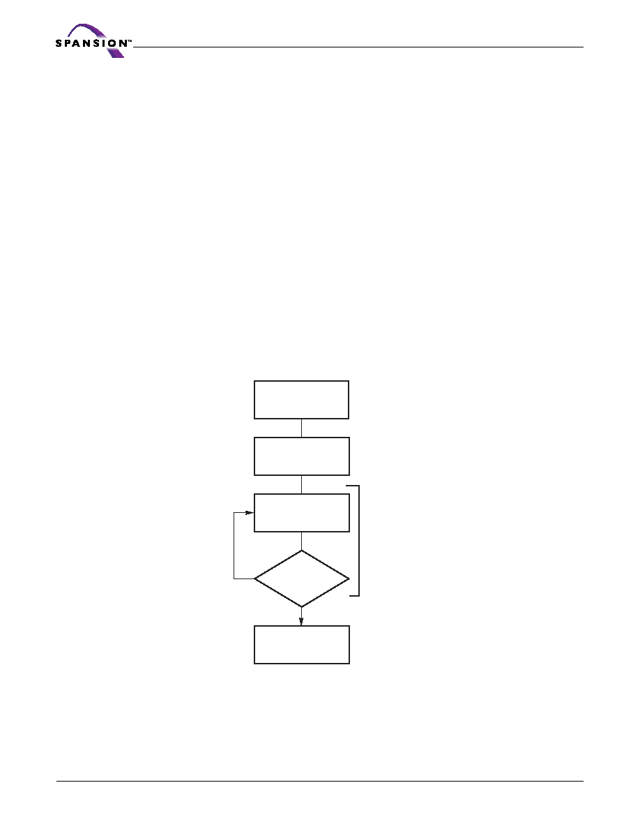
Figure 2 illustrates the algorithm for the program operation. Refer to the Erase/
Program Operations table in the AC Characteristics section for parameters, and
diagrams.
Figure 2. Erase Operation
Chip Erase Command Sequence
Chip erase is a six bus cycle operation. The chip erase command sequence is ini-
tiated by writing two unlock cycles, followed by a set-up command. Two
additional unlock write cycles are then followed by the chip erase command,
which in turn invokes the Embedded Erase algorithm. The device does not require
START
Write Erase
Command Sequence
Data Poll
from System
Data = FFh?
No
Yes
Erasure Completed
Embedded
Erase
algorithm
in progress
相關(guān)PDF資料 |
PDF描述 |
|---|---|
| AM29BDS320GTC8VMF | 2M X 16 FLASH 1.8V PROM, 90 ns, PBGA64 |
| AM29DL163CB70RZCB | 2M X 8 FLASH 3V PROM, 70 ns, PDSO48 |
| AM29DL162CB120WCEB | 2M X 8 FLASH 3V PROM, 120 ns, PBGA48 |
| AM29DL162CB120EIN | 2M X 8 FLASH 3V PROM, 120 ns, PDSO48 |
| AM29DL162CT120EIB | 2M X 8 FLASH 3V PROM, 120 ns, PDSO48 |
相關(guān)代理商/技術(shù)參數(shù) |
參數(shù)描述 |
|---|---|
| AM29BDS643GT5KVAI | 制造商:Spansion 功能描述:FLASH PARALLEL 1.8V 64MBIT 4MX16 55NS 44FBGA - Trays |
| AM29BL802CB-65RZET | 制造商:Spansion 功能描述: |
| AM29C01WW WAF | 制造商:Advanced Micro Devices 功能描述: |
| AM29C10API | 制造商:Rochester Electronics LLC 功能描述:- Bulk |
| AM29C10AWW DIE | 制造商:Advanced Micro Devices 功能描述: |
發(fā)布緊急采購,3分鐘左右您將得到回復(fù)。