- 您現(xiàn)在的位置:買賣IC網(wǎng) > PDF目錄362278 > AM50DL128BG Am50DL128BG - Stacked Multi-Chip Package (MCP) Flash Memory and SRAM PDF資料下載
參數(shù)資料
| 型號: | AM50DL128BG |
| 英文描述: | Am50DL128BG - Stacked Multi-Chip Package (MCP) Flash Memory and SRAM |
| 中文描述: | Am50DL128BG -堆疊式多芯片封裝(MCP)閃存和SRAM |
| 文件頁數(shù): | 44/70頁 |
| 文件大小: | 1042K |
| 代理商: | AM50DL128BG |
第1頁第2頁第3頁第4頁第5頁第6頁第7頁第8頁第9頁第10頁第11頁第12頁第13頁第14頁第15頁第16頁第17頁第18頁第19頁第20頁第21頁第22頁第23頁第24頁第25頁第26頁第27頁第28頁第29頁第30頁第31頁第32頁第33頁第34頁第35頁第36頁第37頁第38頁第39頁第40頁第41頁第42頁第43頁當前第44頁第45頁第46頁第47頁第48頁第49頁第50頁第51頁第52頁第53頁第54頁第55頁第56頁第57頁第58頁第59頁第60頁第61頁第62頁第63頁第64頁第65頁第66頁第67頁第68頁第69頁第70頁
May 19, 2003
Am50DL9608G
43
P R E L I M I N A R Y
ABSOLUTE MAXIMUM RATINGS
Storage Temperature
Plastic Packages . . . . . . . . . . . . . . . –55
°
C to +125
°
C
Ambient Temperature
with Power Applied . . . . . . . . . . . . . . –40
°
C to +85
°
C
Voltage with Respect to Ground
V
CC
(Note 1) . . . . . . . . . . . . . . . . .–0.5 V to +4.0 V
RESET# (Note 2) . . . . . . . . . . . .–0.5 V to +12.5 V
WP#/ACC . . . . . . . . . . . . . . . . . .–0.5 V to +10.5 V
All other pins (Note 1). . . . . . –0.5 V to V
CC
+0.5 V
Output Short Circuit Current (Note 3) . . . . . . 200 mA
Notes:
1. Minimum DC voltage on input or I/O pins is –0.5 V.
During voltage transitions, input or I/O pins may
overshoot V
SS
to –2.0 V for periods of up to 20 ns.
Maximum DC voltage on input or I/O pins is V
CC
+0.5 V.
See Figure 7. During voltage transitions, input or I/O pins
may overshoot to V
CC
+2.0 V for periods up to 20 ns. See
Figure 8.
2. Minimum DC input voltage on pins RESET#, and
WP#/ACC is –0.5 V. During voltage transitions,
WP#/ACC, and RESET# may overshoot V
SS
to –2.0 V
for periods of up to 20 ns. See Figure 7. Maximum DC
input voltage on pin RESET# is +12.5 V which may
overshoot to +14.0 V for periods up to 20 ns. Maximum
DC input voltage on WP#/ACC is +9.5 V which may
overshoot to +12.0 V for periods up to 20 ns.
3. No more than one output may be shorted to ground at a
time. Duration of the short circuit should not be greater
than one second.
Stresses above those listed under “Absolute Maximum
Ratings” may cause permanent damage to the device. This
is a stress rating only; functional operation of the device at
these or any other conditions above those indicated in the
operational sections of this data sheet is not implied.
Exposure of the device to absolute maximum rating
conditions for extended periods may affect device reliability.
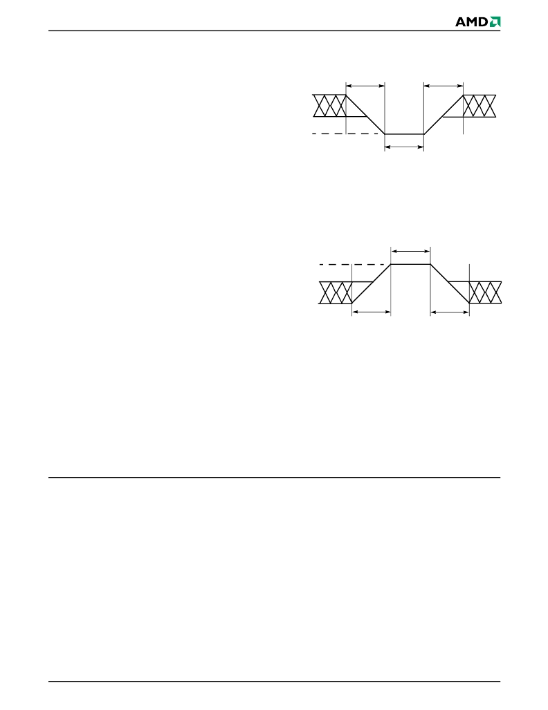
Figure 8.
Overshoot Waveform
Maximum Negative
Figure 9.
Overshoot Waveform
Maximum Positive
OPERATING RANGES
Industrial (I) Devices
Ambient Temperature (T
A
) . . . . . . . . . –40°C to +85°C
V
CC
f/V
CC
s Supply Voltages
V
CC
f/V
CC
s
for standard voltage range . .2.7 V to 3.3 V
Operating ranges define those limits between which the
functionality of the device is guaranteed.
20 ns
20 ns
+0.8 V
–0.5 V
20 ns
–2.0 V
20 ns
20 ns
V
+2.0 V
V
+0.5 V
20 ns
2.0 V
相關PDF資料 |
PDF描述 |
|---|---|
| AM50DL128CG | 2 x 64 Mbit (8 M x 8-Bit/4 M x 16-Bit) CMOS and 64 Mbit (2 M x 16-Bit) Pseudo Static RAM (Preliminary) |
| AM50DL128CH | Am50DL128CH - Stacked Multi-Chip Package (MCP) Flash Memory and SRAM |
| AM52-0001 | 1.2 W High Efficiency Power Amplifier 800 - 960 MHz |
| AM52-0001SMB | 1.2 W High Efficiency Power Amplifier 800 - 960 MHz |
| AM52-0001TR | 1.2 W High Efficiency Power Amplifier 800 - 960 MHz |
相關代理商/技術參數(shù) |
參數(shù)描述 |
|---|---|
| AM50DL128BG70I | 制造商:Spansion 功能描述:Combo Mem 4Mx16/8Mx8 Flash + 2Mx16 PSRAM 3V 73-Pin FBGA |
| AM50DL128BG85I | 制造商:Spansion 功能描述:COMBO 4MX16/8MX8 FLASH + 2MX16 PSRAM 3V/3.3V 73FBGA - Trays |
| AM50DL128BH | 制造商:AMD 制造商全稱:Advanced Micro Devices 功能描述:Stacked Multi-Chip Package (MCP) Flash Memory and SRAM |
| AM50DL128BH_04 | 制造商:SPANSION 制造商全稱:SPANSION 功能描述:Two Am29DL640G 64 Megabit (8 M x 8-Bit/4 M x 16-Bit) CMOS 3.0 Volt-only, Simultaneous Operation Flash Memories |
| AM50DL128BH56I | 制造商:AMD 制造商全稱:Advanced Micro Devices 功能描述:Stacked Multi-Chip Package (MCP) Flash Memory and SRAM |
發(fā)布緊急采購,3分鐘左右您將得到回復。