- 您現(xiàn)在的位置:買賣IC網(wǎng) > PDF目錄170346 > CY7C1350-133ACT (CYPRESS SEMICONDUCTOR CORP) 128K X 36 ZBT SRAM, 4.2 ns, PQFP100 PDF資料下載
參數(shù)資料
| 型號: | CY7C1350-133ACT |
| 廠商: | CYPRESS SEMICONDUCTOR CORP |
| 元件分類: | SRAM |
| 英文描述: | 128K X 36 ZBT SRAM, 4.2 ns, PQFP100 |
| 封裝: | 14 X 20 MM, 1.40 MM HEIGHT, PLASTIC, TQFP-100 |
| 文件頁數(shù): | 1/13頁 |
| 文件大小: | 187K |
| 代理商: | CY7C1350-133ACT |
128Kx36 Pipelined SRAM with NoBL Architecture
CY7C1350
Cypress Semiconductor Corporation
3901 North First Street
San Jose
CA 95134
408-943-2600
August 9, 1999
Features
Pin compatible and functionally equivalent to ZBT de-
vices IDT71V546, MT55L128L36P, and MCM63Z736
Supports 143-MHz bus operations with zero wait states
— Data is transferred on every clock
Internally self-timed output buffer control to eliminate
the need to use OE
Fully registered (inputs and outputs) for pipelined
operation
Byte Write capability
128K x 36 common I/O architecture
Single 3.3V power supply
Fast clock-to-output times
— 4.0 ns (for 143-MHz device)
— 4.2 ns (for 133-MHz device)
— 5.0 ns (for 100-MHz device)
— 7.0 ns (for 80-MHz device)
Clock Enable (CEN) pin to suspend operation
Synchronous self-timed writes
Asynchronous output enable
JEDEC-standard 100 TQFP package
Burst Capability — linear or interleaved burst order
Low standby power (17.325 mW max.)
Functional Description
The CY7C1350 is a 3.3V, 128K by 36 synchronous-pipelined
Burst SRAM designed specifically to support unlimited true
back-to-back Read/Write operations without the insertion of
wait states. The CY7C1350 is equipped with the advanced No
Bus Latency (NoBL) logic required to enable consecutive
Read/Write operations with data being transferred on every
clock cycle. This feature dramatically improves the throughput
of the SRAM, especially in systems that require frequent
Write/Read transitions. The CY7C1350 is pin/functionally
compatible to ZBT SRAMs IDT71V546, MT55L128L36P,
and MCM63Z736.
All synchronous inputs pass through input registers controlled
by the rising edge of the clock. All data outputs pass through
output registers controlled by the rising edge of the clock. The
clock input is qualified by the Clock Enable (CEN) signal, which
when deasserted suspends operation and extends the previ-
ous clock cycle. Maximum access delay from the clock rise is
4.0 ns (143-MHz device).
Write operations are controlled by the four Byte Write Select
(BWS[3:0]) and a Write Enable (WE) input. All writes are con-
ducted with on-chip synchronous self-timed write circuitry.
Three synchronous Chip Enables (CE1, CE2, CE3) and an
asynchronous Output Enable (OE) provide for easy bank se-
lection and output three-state control. In order to avoid bus
contention, the output drivers are synchronously three-stated
during the data portion of a write sequence.
.
NoBLand No Bus Latency are trademarks of Cypress Semiconductor Corporation.
ZBT is a trademark of Integrated Device Technology.
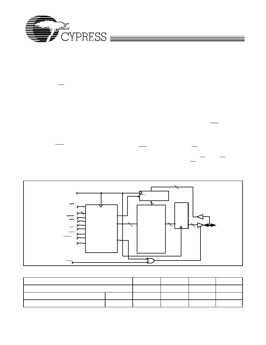
CLK
A[16:0]
CEN
WE
BWS[3:0]
CE1
CE
CE2
OE
OOUT
P
UT
128Kx36
MEMORY
ARRAY
CL
K
Logic Block Diagram
DQ[31:0]
Data-In REG.
Q
D
CE
CONTROL
and WRITE
LOGIC
3
R
E
G
ISTER
S
an
d
LO
G
IC
ADV/LD
36
17
36
DP[3:0]
MODE
Selection Guide
7C1350-143
7C1350-133
7C1350-100
7C1350-80
Maximum Access Time (ns)
4.0
4.2
5.0
7.0
Maximum Operating Current (mA)
Commercial
450
400
350
300
Maximum CMOS Standby Current (mA)
Commercial
5
相關(guān)PDF資料 |
PDF描述 |
|---|---|
| CY7C1425BV18-200BZXC | 4M X 9 QDR SRAM, 0.45 ns, PBGA165 |
| CY7C1442AV25-200BZC | 2M X 18 CACHE SRAM, 3.2 ns, PBGA165 |
| CY7C1561KV18-500BZI | 8M X 8 QDR SRAM, 0.33 ns, PBGA165 |
| CY7C172A-25VC | 4K X 4 STANDARD SRAM, 25 ns, PDSO24 |
| CY7C188-35VC | 32K X 9 STANDARD SRAM, 35 ns, PDSO32 |
相關(guān)代理商/技術(shù)參數(shù) |
參數(shù)描述 |
|---|---|
| CY7C1350-133AXC | 制造商:Cypress Semiconductor 功能描述: |
| CY7C1350B-133AC | 制造商:Cypress Semiconductor 功能描述:SRAM Chip Sync Single 3.3V 4.5M-Bit 128K x 36 4.2ns 100-Pin TQFP |
| CY7C1350B-133AI | 制造商:Rochester Electronics LLC 功能描述:- Bulk |
| CY7C1350F-133AI | 制造商:Cypress Semiconductor 功能描述: |
| CY7C1350F-200AC | 制造商:Cypress Semiconductor 功能描述:SRAM Chip Sync Single 3.3V 4.5M-Bit 128K x 36 2.8ns 100-Pin TQFP |
發(fā)布緊急采購,3分鐘左右您將得到回復(fù)。