- 您現(xiàn)在的位置:買賣IC網(wǎng) > PDF目錄170347 > CY7C1561KV18-500BZI (CYPRESS SEMICONDUCTOR CORP) 8M X 8 QDR SRAM, 0.33 ns, PBGA165 PDF資料下載
參數(shù)資料
| 型號(hào): | CY7C1561KV18-500BZI |
| 廠商: | CYPRESS SEMICONDUCTOR CORP |
| 元件分類: | SRAM |
| 英文描述: | 8M X 8 QDR SRAM, 0.33 ns, PBGA165 |
| 封裝: | 15 X 13 MM, 1.4 MM HEIGHT, FBGA-165 |
| 文件頁數(shù): | 25/28頁 |
| 文件大小: | 827K |
| 代理商: | CY7C1561KV18-500BZI |
第1頁第2頁第3頁第4頁第5頁第6頁第7頁第8頁第9頁第10頁第11頁第12頁第13頁第14頁第15頁第16頁第17頁第18頁第19頁第20頁第21頁第22頁第23頁第24頁當(dāng)前第25頁第26頁第27頁第28頁
PRELIMINARY
CY7C1561KV18, CY7C1576KV18
CY7C1563KV18, CY7C1565KV18
Document Number: 001-15878 Rev. *E
Page 6 of 28
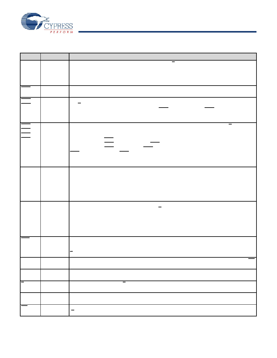
Pin Definitions
Pin Name
I/O
Pin Description
D[x:0]
Input-
Synchronous
Data Input Signals. Sampled on the rising edge of K and K clocks when valid write operations are active.
CY7C1561KV18
D[7:0]
CY7C1576KV18
D[8:0]
CY7C1563KV18
D[17:0]
CY7C1565KV18
D[35:0]
WPS
Input-
Synchronous
Write Port Select
Active LOW. Sampled on the rising edge of the K clock. When asserted active, a
write operation is initiated. Deasserting deselects the write port. Deselecting the write port ignores D[x:0].
NWS0,
NWS1,
Input-
Synchronous
Nibble Write Select 0, 1
Active LOW (CY7C1561KV18 Only). Sampled on the rising edge of the K
and K clocks when write operations are active. Used to select which nibble is written into the device
during the current portion of the write operations. NWS0 controls D[3:0] and NWS1 controls D[7:4].
All the Nibble Write Selects are sampled on the same edge as the data. Deselecting a Nibble Write Select
ignores the corresponding nibble of data and it is not written into the device.
BWS0,
BWS1,
BWS2,
BWS3
Input-
Synchronous
Byte Write Select 0, 1, 2, and 3
Active LOW. Sampled on the rising edge of the K and K clocks when
write operations are active. Used to select which byte is written into the device during the current portion
of the write operations. Bytes not written remain unaltered.
CY7C1576KV18
BWS0 controls D[8:0]
CY7C1563KV18
BWS0 controls D[8:0] and BWS1 controls D[17:9].
CY7C1565KV18
BWS0 controls D[8:0], BWS1 controls D[17:9],
BWS2 controls D[26:18] and BWS3 controls D[35:27].
All the Byte Write Selects are sampled on the same edge as the data. Deselecting a Byte Write Select
ignores the corresponding byte of data and it is not written into the device.
A
Input-
Synchronous
Address Inputs. Sampled on the rising edge of the K clock during active read and write operations. These
address inputs are multiplexed for both read and write operations. Internally, the device is organized as
8M x 8 (4 arrays each of 2M x 8) for CY7C1561KV18, 8M x 9 (4 arrays each of 2M x 9) for CY7C1576KV18,
4M x 18 (4 arrays each of 1M x 18) for CY7C1563KV18 and 2M x 36 (4 arrays each of 512K x 36) for
CY7C1565KV18. Therefore, only 21 address inputs are needed to access the entire memory array of
CY7C1561KV18 and CY7C1576KV18, 20 address inputs for CY7C1563KV18 and 19 address inputs for
CY7C1565KV18. These inputs are ignored when the appropriate port is deselected.
Q[x:0]
Outputs-
Synchronous
Data Output Signals. These pins drive out the requested data when the read operation is active. Valid
data is driven out on the rising edge of the K and K clocks during read operations. On deselecting the
read port, Q[x:0] are automatically tristated.
CY7C1561KV18
Q[7:0]
CY7C1576KV18
Q[8:0]
CY7C1563KV18
Q[17:0]
CY7C1565KV18
Q[35:0]
RPS
Input-
Synchronous
Read Port Select
Active LOW. Sampled on the rising edge of positive input clock (K). When active, a
read operation is initiated. Deasserting deselects the read port. When deselected, the pending access is
allowed to complete and the output drivers are automatically tristated following the next rising edge of the
K clock. Each read access consists of a burst of four sequential transfers.
QVLD
Valid output
indicator
Valid Output Indicator. The Q Valid indicates valid output data. QVLD is edge aligned with CQ and CQ.
K
Input Clock
Positive Input Clock Input. The rising edge of K is used to capture synchronous inputs to the device
and to drive out data through Q[x:0]. All accesses are initiated on the rising edge of K.
K
Input Clock
Negative Input Clock Input. K is used to capture synchronous inputs being presented to the device and
to drive out data through Q[x:0].
CQ
Echo Clock
Synchronous Echo Clock Outputs. This is a free running clock and is synchronized to the input clock
(K) of the QDR-II+. The timings for the echo clocks are shown in the Switching Characteristics on page 23.
CQ
Echo Clock
Synchronous Echo Clock Outputs. This is a free running clock and is synchronized to the input clock
(K) of the QDR-II+.The timings for the echo clocks are shown in the Switching Characteristics on page 23.
相關(guān)PDF資料 |
PDF描述 |
|---|---|
| CY7C172A-25VC | 4K X 4 STANDARD SRAM, 25 ns, PDSO24 |
| CY7C188-35VC | 32K X 9 STANDARD SRAM, 35 ns, PDSO32 |
| CY7C292A-25DI | 2K X 8 OTPROM, 25 ns, CDIP24 |
| CY7C43663-12AI | 4K X 36 OTHER FIFO, 9 ns, PQFP128 |
| CY8C3444AXI-116 | MULTIFUNCTION PERIPHERAL, PQFP100 |
相關(guān)代理商/技術(shù)參數(shù) |
參數(shù)描述 |
|---|---|
| CY7C1562XV18-366BZC | 功能描述:靜態(tài)隨機(jī)存取存儲(chǔ)器 72MB (4Mx18) 1.8v 366MHz QDR II 靜態(tài)隨機(jī)存取存儲(chǔ)器 RoHS:否 制造商:Cypress Semiconductor 存儲(chǔ)容量:16 Mbit 組織:1 M x 16 訪問時(shí)間:55 ns 電源電壓-最大:3.6 V 電源電壓-最小:2.2 V 最大工作電流:22 uA 最大工作溫度:+ 85 C 最小工作溫度:- 40 C 安裝風(fēng)格:SMD/SMT 封裝 / 箱體:TSOP-48 封裝:Tray |
| CY7C1562XV18-366BZXC | 功能描述:靜態(tài)隨機(jī)存取存儲(chǔ)器 72MB (4Mx18) 1.8v 366MHz QDR II 靜態(tài)隨機(jī)存取存儲(chǔ)器 RoHS:否 制造商:Cypress Semiconductor 存儲(chǔ)容量:16 Mbit 組織:1 M x 16 訪問時(shí)間:55 ns 電源電壓-最大:3.6 V 電源電壓-最小:2.2 V 最大工作電流:22 uA 最大工作溫度:+ 85 C 最小工作溫度:- 40 C 安裝風(fēng)格:SMD/SMT 封裝 / 箱體:TSOP-48 封裝:Tray |
| CY7C1562XV18-450BZC | 功能描述:靜態(tài)隨機(jī)存取存儲(chǔ)器 72MB (4Mx18) 1.8v 450MHz QDR II 靜態(tài)隨機(jī)存取存儲(chǔ)器 RoHS:否 制造商:Cypress Semiconductor 存儲(chǔ)容量:16 Mbit 組織:1 M x 16 訪問時(shí)間:55 ns 電源電壓-最大:3.6 V 電源電壓-最小:2.2 V 最大工作電流:22 uA 最大工作溫度:+ 85 C 最小工作溫度:- 40 C 安裝風(fēng)格:SMD/SMT 封裝 / 箱體:TSOP-48 封裝:Tray |
| CY7C1562XV18-450BZXC | 功能描述:靜態(tài)隨機(jī)存取存儲(chǔ)器 72MB (4Mx18) 1.8v 450MHz QDR II 靜態(tài)隨機(jī)存取存儲(chǔ)器 RoHS:否 制造商:Cypress Semiconductor 存儲(chǔ)容量:16 Mbit 組織:1 M x 16 訪問時(shí)間:55 ns 電源電壓-最大:3.6 V 電源電壓-最小:2.2 V 最大工作電流:22 uA 最大工作溫度:+ 85 C 最小工作溫度:- 40 C 安裝風(fēng)格:SMD/SMT 封裝 / 箱體:TSOP-48 封裝:Tray |
| CY7C15631KV18450BZC | 制造商:Cypress Semiconductor 功能描述:CY7C15631KV18-450BZC |
發(fā)布緊急采購,3分鐘左右您將得到回復(fù)。