- 您現(xiàn)在的位置:買賣IC網(wǎng) > PDF目錄362688 > EM78P569 (ELAN Microelctronics Corp .) 8 - BIT OTP MICRO CONTROLLER PDF資料下載
參數(shù)資料
| 型號: | EM78P569 |
| 廠商: | ELAN Microelctronics Corp . |
| 英文描述: | 8 - BIT OTP MICRO CONTROLLER |
| 中文描述: | 8 -位微控制器檢察官辦公室 |
| 文件頁數(shù): | 13/58頁 |
| 文件大小: | 475K |
| 代理商: | EM78P569 |
第1頁第2頁第3頁第4頁第5頁第6頁第7頁第8頁第9頁第10頁第11頁第12頁當(dāng)前第13頁第14頁第15頁第16頁第17頁第18頁第19頁第20頁第21頁第22頁第23頁第24頁第25頁第26頁第27頁第28頁第29頁第30頁第31頁第32頁第33頁第34頁第35頁第36頁第37頁第38頁第39頁第40頁第41頁第42頁第43頁第44頁第45頁第46頁第47頁第48頁第49頁第50頁第51頁第52頁第53頁第54頁第55頁第56頁第57頁第58頁
EM78P569
8-bit OTP Micro-controller
__________________________________________________________________________________________________________________________________________________________________
* This specification is subject to be changed without notice.
8/19/2004 V4.4
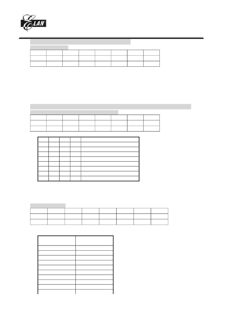
R4 (RAM selection for common registers R20 ~ R3F))
(RAM selection register)
7
6
5
RB1
RB0
RSR5
R/W-0
R/W-0
R/W
Bit 0 ~ Bit 5 (RSR0 ~ RSR5) : Indirect addressing for common registers R20 ~ R3F
RSR bits are used to select up to 32 registers (R20 to R3F) in the indirect addressing mode.
Bit 6 ~ Bit 7 (RB0 ~ RB1) : Bank selection bits for common registers R20 ~ R3F
These selection bits are used to determine which bank is activated among the 4 banks for 32 register (R20 to
R3F)..
Please refer to VII.1 Operational registers for details.
4
3
2
1
0
RSR4
R/W
RSR3
R/W
RSR2
R/W
RSR1
R/W
RSR0
R/W
R5 (PORT5 I/O data, Program page selection, LCD address, SPI control, PWM control)
PAGE0 (PORT5 I/O data register, Program page register)
7
6
5
4
3
P57
P56
P55
-
PS3
R/W
R/W
R/W
R/W-0
Bit 0 ~ Bit 3 (PS0 ~ PS3) : Program page selection bits
PS3
PS2
PS1
PS0
Program memory page (Address)
0
0
0
0
Page 0
0
0
0
1
Page 1
0
0
1
0
Page 2
0
0
1
1
Page 3
:
:
:
:
:
:
:
:
:
:
1
1
1
0
Page 14
1
1
1
1
Page 15
User can use PAGE instruction to change page to maintain program page by user.
Bit 4 :
(undefined) not allowed to use
Bit 5 ~ Bit 7 (P55 ~ P57) : 8-bit PORT5(5~7) I/O data register
User can use IOC register to define input or output each bit.
PAGE1 (LCD address)
7
6
5
4
3
DA9
DA8
-
-
LCDA3
R/W
R/W
R/W-0
Bit 0 ~ Bit 3 (LCDA0 ~ LCDA3) : LCD address for LCD RAM read or write
The address of the LCD RAM correspond to the COMMON and SEGMENT signals as the table.
COM3 ~ COM0
LCD address
(LCDA3 ~ LCDA0)
SEG1, SEG0
00H
SEG3, SEG2
01H
SEG5, SEG4
02H
SEG7, SEG6
03H
SEG9, SEG8
04H
SEG11, SEG10
05H
SEG13, SEG12
06H
SEG15, SEG14
07H
SEG17, SEG16
08H
SEG19, SEG18
09H
2
1
0
PS2
R/W-0
PS1
R/W-0
PS0
R/W-0
2
1
0
LCDA2
R/W-0
LCDA1
R/W-0
LCDA0
R/W-0
相關(guān)PDF資料 |
PDF描述 |
|---|---|
| EM78P5840 | 8 BIT MICROCONTROLLER |
| EM78P5841 | 8 BIT MICROCONTROLLER |
| EM78P5842 | 8 BIT MICROCONTROLLER |
| EM78P809N | 8-BIT MICROCONTROLLER |
| EM78P809NM | 8-BIT MICROCONTROLLER |
相關(guān)代理商/技術(shù)參數(shù) |
參數(shù)描述 |
|---|---|
| EM7A8620 | 制造商:EMC 制造商全稱:ELAN Microelectronics Corp 功能描述:Voice over IP |
| EM7G | 制造商:GULFSEMI 制造商全稱:Gulf Semiconductor 功能描述:ULTRAFAST EFFICIENT PLASTIC SILICON RECTIFIER VOLTAGE: 1000V CURRENT: 1.0A |
| EM800 | 制造商:EDI 制造商全稱:Electronic devices inc. 功能描述:HIGH VOLTAGE HIGH CURRENT MINIATURE RECTIFIERS |
| EM8000EHP | 制造商:JDSU 制造商全稱:JDS Uniphase Corporation 功能描述:The industrya??s most compact 100 G test solution |
| EM800-DCM | 制造商:MRV 制造商全稱:MRV 功能描述:LambdaDriver Dispersion Compensation Module (EM800/1600-DCM and DCMD) |
發(fā)布緊急采購,3分鐘左右您將得到回復(fù)。