- 您現(xiàn)在的位置:買賣IC網(wǎng) > PDF目錄362688 > EM78P569 (ELAN Microelctronics Corp .) 8 - BIT OTP MICRO CONTROLLER PDF資料下載
參數(shù)資料
| 型號: | EM78P569 |
| 廠商: | ELAN Microelctronics Corp . |
| 英文描述: | 8 - BIT OTP MICRO CONTROLLER |
| 中文描述: | 8 -位微控制器檢察官辦公室 |
| 文件頁數(shù): | 42/58頁 |
| 文件大?。?/td> | 475K |
| 代理商: | EM78P569 |
第1頁第2頁第3頁第4頁第5頁第6頁第7頁第8頁第9頁第10頁第11頁第12頁第13頁第14頁第15頁第16頁第17頁第18頁第19頁第20頁第21頁第22頁第23頁第24頁第25頁第26頁第27頁第28頁第29頁第30頁第31頁第32頁第33頁第34頁第35頁第36頁第37頁第38頁第39頁第40頁第41頁當(dāng)前第42頁第43頁第44頁第45頁第46頁第47頁第48頁第49頁第50頁第51頁第52頁第53頁第54頁第55頁第56頁第57頁第58頁
EM78P569
8-bit OTP Micro-controller
__________________________________________________________________________________________________________________________________________________________________
* This specification is subject to be changed without notice.
8/19/2004 V4.4
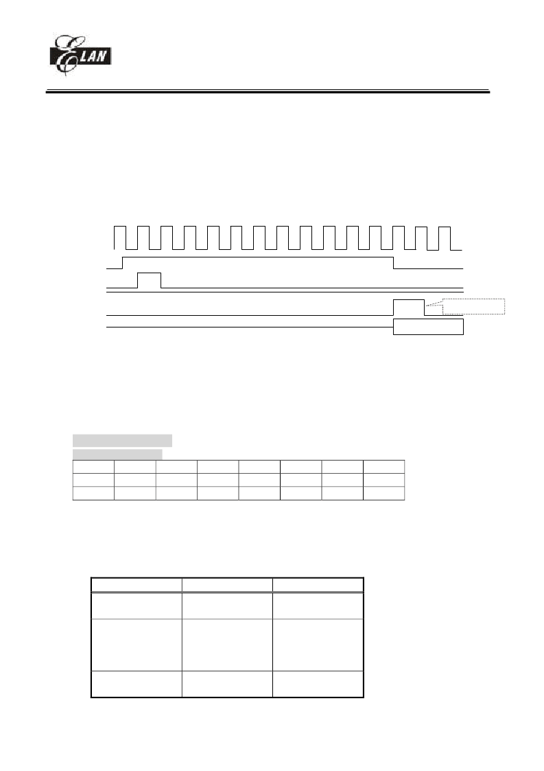
If ADI = 0 in IOCE PAGE0 Bit5, when A/D start conversion by setting ADST(IOCB PAGE1 Bit0) = 1 then
A/D will continue conversion without stop and hardware won’t reset ADST bit. In this condition, ADI is
deactived. After ADI in IOCE PAGE0 bit5 is set, ADI in RE PAGE0 bit5 will activate again.
To minimum operating current , all biasing circuits in the A/D module that consume DC current are power
down when ADPWR bit in IOCB PAGE1 Bit2 register is a ’0’. When ADPWR bit is a ‘1’, A/D converter
module is operating.
User has to set PORT60~ PORT65as AD converter input pin or bi-direction IO PORT.
Fig.15 A/D converter timing
Bit 6 (RBF) : SPI’s RBF interrupt mask
0/1
disable/enable interrupt
Bit 7 (PWM2) : PWM2 interrupt enable bit
0/1
disable/enable interrupt
IOCF (Interrupt mask)
(Interrupt mask register)
Bit7
INT3
R/W-0
R/W-0
Bit 0 ~ 5,7 : interrupt enable bit
0
disable interrupt
1
enable interrupt
Bit 6
: (remain these values to “0”othwise it will generate unpredicted interrupts)
The status after interrupt and the interrupt sources list as the table below.
Interrupt signal
GREEN mode
RA(7,6)=(x,0)
no SLEP
TCC time out
IOCF bit0=1
And "ENI"
COUNTER1 time out
IOCF bit1=1
(jump to address 8 at
Bit6
0
Bit5
INT2
R/W-0
Bit4
INT1
R/W-0
Bit3
INT0
R/W-0
Bit2
CNT2
R/W-0
Bit1
CNT1
R/W-0
Bit0
TCIF
R/W-0
NORMAL mode
RA(7,6)=(x,1)
no SLEP
Interrupt
(jump to address 8 at
page0)
Interrupt
(jump to address 8 at
page0)
Interrupt
Interrupt
(jump to address 8 at
START
SAMPLE
ADI(IOCE PAGE0 bit5 ) =1
ADI(RE PAGE0 bit 5)
DATA
Clear by software
1
2
3
4
5
6
7
8
9
10
11
12
相關(guān)PDF資料 |
PDF描述 |
|---|---|
| EM78P5840 | 8 BIT MICROCONTROLLER |
| EM78P5841 | 8 BIT MICROCONTROLLER |
| EM78P5842 | 8 BIT MICROCONTROLLER |
| EM78P809N | 8-BIT MICROCONTROLLER |
| EM78P809NM | 8-BIT MICROCONTROLLER |
相關(guān)代理商/技術(shù)參數(shù) |
參數(shù)描述 |
|---|---|
| EM7A8620 | 制造商:EMC 制造商全稱:ELAN Microelectronics Corp 功能描述:Voice over IP |
| EM7G | 制造商:GULFSEMI 制造商全稱:Gulf Semiconductor 功能描述:ULTRAFAST EFFICIENT PLASTIC SILICON RECTIFIER VOLTAGE: 1000V CURRENT: 1.0A |
| EM800 | 制造商:EDI 制造商全稱:Electronic devices inc. 功能描述:HIGH VOLTAGE HIGH CURRENT MINIATURE RECTIFIERS |
| EM8000EHP | 制造商:JDSU 制造商全稱:JDS Uniphase Corporation 功能描述:The industrya??s most compact 100 G test solution |
| EM800-DCM | 制造商:MRV 制造商全稱:MRV 功能描述:LambdaDriver Dispersion Compensation Module (EM800/1600-DCM and DCMD) |
發(fā)布緊急采購,3分鐘左右您將得到回復(fù)。