- 您現(xiàn)在的位置:買(mǎi)賣(mài)IC網(wǎng) > PDF目錄11581 > ENC424J600T-I/PT (Microchip Technology)IC ETHERNET CTRLR W/SPI 44-TQFP PDF資料下載
參數(shù)資料
| 型號(hào): | ENC424J600T-I/PT |
| 廠商: | Microchip Technology |
| 文件頁(yè)數(shù): | 96/168頁(yè) |
| 文件大小: | 0K |
| 描述: | IC ETHERNET CTRLR W/SPI 44-TQFP |
| 視頻文件: | Fast 100 Mbps Ethernet PICtail Plus Overview |
| 標(biāo)準(zhǔn)包裝: | 1,200 |
| 控制器類(lèi)型: | 以太網(wǎng)控制器(IEEE 802.3) |
| 接口: | SPI |
| 電源電壓: | 3 V ~ 3.6 V |
| 電流 - 電源: | 96mA |
| 工作溫度: | -40°C ~ 85°C |
| 安裝類(lèi)型: | 表面貼裝 |
| 封裝/外殼: | 44-TQFP |
| 供應(yīng)商設(shè)備封裝: | 44-TQFP(10x10) |
| 包裝: | 帶卷 (TR) |
| 配用: | AC164132-ND - BOARD DAUGHTER PICTAIL ETHERNET |
第1頁(yè)第2頁(yè)第3頁(yè)第4頁(yè)第5頁(yè)第6頁(yè)第7頁(yè)第8頁(yè)第9頁(yè)第10頁(yè)第11頁(yè)第12頁(yè)第13頁(yè)第14頁(yè)第15頁(yè)第16頁(yè)第17頁(yè)第18頁(yè)第19頁(yè)第20頁(yè)第21頁(yè)第22頁(yè)第23頁(yè)第24頁(yè)第25頁(yè)第26頁(yè)第27頁(yè)第28頁(yè)第29頁(yè)第30頁(yè)第31頁(yè)第32頁(yè)第33頁(yè)第34頁(yè)第35頁(yè)第36頁(yè)第37頁(yè)第38頁(yè)第39頁(yè)第40頁(yè)第41頁(yè)第42頁(yè)第43頁(yè)第44頁(yè)第45頁(yè)第46頁(yè)第47頁(yè)第48頁(yè)第49頁(yè)第50頁(yè)第51頁(yè)第52頁(yè)第53頁(yè)第54頁(yè)第55頁(yè)第56頁(yè)第57頁(yè)第58頁(yè)第59頁(yè)第60頁(yè)第61頁(yè)第62頁(yè)第63頁(yè)第64頁(yè)第65頁(yè)第66頁(yè)第67頁(yè)第68頁(yè)第69頁(yè)第70頁(yè)第71頁(yè)第72頁(yè)第73頁(yè)第74頁(yè)第75頁(yè)第76頁(yè)第77頁(yè)第78頁(yè)第79頁(yè)第80頁(yè)第81頁(yè)第82頁(yè)第83頁(yè)第84頁(yè)第85頁(yè)第86頁(yè)第87頁(yè)第88頁(yè)第89頁(yè)第90頁(yè)第91頁(yè)第92頁(yè)第93頁(yè)第94頁(yè)第95頁(yè)當(dāng)前第96頁(yè)第97頁(yè)第98頁(yè)第99頁(yè)第100頁(yè)第101頁(yè)第102頁(yè)第103頁(yè)第104頁(yè)第105頁(yè)第106頁(yè)第107頁(yè)第108頁(yè)第109頁(yè)第110頁(yè)第111頁(yè)第112頁(yè)第113頁(yè)第114頁(yè)第115頁(yè)第116頁(yè)第117頁(yè)第118頁(yè)第119頁(yè)第120頁(yè)第121頁(yè)第122頁(yè)第123頁(yè)第124頁(yè)第125頁(yè)第126頁(yè)第127頁(yè)第128頁(yè)第129頁(yè)第130頁(yè)第131頁(yè)第132頁(yè)第133頁(yè)第134頁(yè)第135頁(yè)第136頁(yè)第137頁(yè)第138頁(yè)第139頁(yè)第140頁(yè)第141頁(yè)第142頁(yè)第143頁(yè)第144頁(yè)第145頁(yè)第146頁(yè)第147頁(yè)第148頁(yè)第149頁(yè)第150頁(yè)第151頁(yè)第152頁(yè)第153頁(yè)第154頁(yè)第155頁(yè)第156頁(yè)第157頁(yè)第158頁(yè)第159頁(yè)第160頁(yè)第161頁(yè)第162頁(yè)第163頁(yè)第164頁(yè)第165頁(yè)第166頁(yè)第167頁(yè)第168頁(yè)
2007 Microchip Technology Inc.
DS21993C-page 31
PIC16CR7X
4.0
I/O PORTS
Some pins for these I/O ports are multiplexed with an
alternate function for the peripheral features on the
device. In general, when a peripheral is enabled, that
pin may not be used as a general purpose I/O pin.
Additional information on I/O ports may be found in the
“PIC Mid-Range MCU Family Reference Manual”
(DS33023).
4.1
PORTA and the TRISA Register
PORTA is a 6-bit wide, bidirectional port. The corre-
sponding data direction register is TRISA. Setting a
TRISA bit (= 1) will make the corresponding PORTA pin
an input (i.e., put the corresponding output driver in a
High-Impendance mode). Clearing a TRISA bit (= 0)
will make the corresponding PORTA pin an output (i.e.,
put the contents of the output latch on the selected pin).
Reading the PORTA register reads the status of the
pins, whereas writing to it will write to the PORT latch.
All write operations are read-modify-write operations.
Therefore, a write to a port implies that the port pins are
read, the value is modified and then written to the
PORT data latch.
Pin RA4 is multiplexed with the Timer0 module clock
input to become the RA4/T0CKI pin. The RA4/T0CKI
pin is a Schmitt Trigger input and an open drain output.
All other PORTA pins have TTL input levels and full
CMOS output drivers.
Other PORTA pins are multiplexed with analog inputs
and analog VREF input. The operation of each pin is
selected by clearing/setting the control bits in the
ADCON1 register (A/D Control Register1).
The TRISA register controls the direction of the RA
pins, even when they are being used as analog inputs.
The user must ensure the bits in the TRISA register are
maintained set, when using them as analog inputs.
EXAMPLE 4-1:
INITIALIZING PORTA
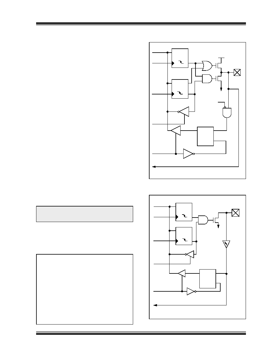
FIGURE 4-1:
BLOCK DIAGRAM OF
RA3:RA0 AND RA5 PINS
FIGURE 4-2:
BLOCK DIAGRAM OF
RA4/T0CKI PIN
Note:
On a Power-on Reset, these pins are
configured as analog inputs and read as
‘0’.
BCF
STATUS, RP0
;
BCF
STATUS, RP1
; Bank0
CLRF
PORTA
; Initialize PORTA by
; clearing output
; data latches
BSF
STATUS, RP0
; Select Bank 1
MOVLW
0x06
; Configure all pins
MOVWF
ADCON1
; as digital inputs
MOVLW
0xCF
; Value used to
; initialize data
; direction
MOVWF
TRISA
; Set RA<3:0> as inputs
; RA<5:4> as outputs
; TRISA<7:6>are always
; read as ‘0’.
Data Bus
P
N
WR Port
WR TRIS
RD TRIS
RD PORT
VSS
VDD
I/O pin(1)
Note
1:
I/O pins have protection diodes to VDD and VSS.
Analog
Input
Mode
TTL
Input
Buffer
To A/D Converter
EN
QD
EN
Data Latch
TRIS Latch
Q
D
Q
CK
Q
D
Q
CK
Data Bus
WR PORT
WR TRIS
RD PORT
Data Latch
TRIS Latch
RD TRIS
Schmitt
Trigger
Input
Buffer
N
VSS
I/O pin(1)
TMR0 Clock Input
Q
D
Q
CK
Q
D
Q
CK
EN
QD
EN
Note
1:
I/O pin has protection diodes to VSS only.
相關(guān)PDF資料 |
PDF描述 |
|---|---|
| PIC16LC505T-04I/SL | IC MCU OTP 1KX12 14SOIC |
| PIC16C620A-04/SS | IC MCU OTP 512X14 COMP 20SSOP |
| PIC16C620A-04I/SS | IC MCU OTP 512X14 COMP 20SSOP |
| PIC12LCE519T-04/SM | IC MCU OTP 1KX12 LV W/EE 8-SOIJ |
| MCP2510T-I/ST | IC CAN CONTROLLER W/SPI 20-TSSOP |
相關(guān)代理商/技術(shù)參數(shù) |
參數(shù)描述 |
|---|---|
| ENC431D05A | 制造商:未知廠家 制造商全稱(chēng):未知廠家 功能描述: |
| ENC431D-05A | 制造商:未知廠家 制造商全稱(chēng):未知廠家 功能描述:STD MOV |
| ENC431D07A | 制造商:未知廠家 制造商全稱(chēng):未知廠家 功能描述: |
| ENC431D-07A | 制造商:未知廠家 制造商全稱(chēng):未知廠家 功能描述:STD MOV |
| ENC431D10A | 制造商:未知廠家 制造商全稱(chēng):未知廠家 功能描述: |
發(fā)布緊急采購(gòu),3分鐘左右您將得到回復(fù)。