- 您現(xiàn)在的位置:買賣IC網(wǎng) > PDF目錄382968 > FS6261-01 (Electronic Theatre Controls, Inc.) Motherboard Clock Generator IC PDF資料下載
參數(shù)資料
| 型號: | FS6261-01 |
| 廠商: | Electronic Theatre Controls, Inc. |
| 英文描述: | Motherboard Clock Generator IC |
| 中文描述: | 主板時(shí)鐘發(fā)生器IC |
| 文件頁數(shù): | 10/17頁 |
| 文件大?。?/td> | 216K |
| 代理商: | FS6261-01 |
XT
January 2000
1.31.00
10
)6
0RWKHUERDUG&ORFN*HQHUDWRU,&
,62
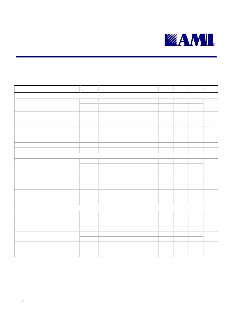
Table 8: DC Electrical Specifications, continued
Unless otherwise stated, all power supplies = 3.3V ± 10%, no load on any output, and ambient temperature range T
= 0°C to 70°C. Parameters denoted with an asterisk ( * ) represent nominal
characterization data and are not currently production tested to any specific limits. MIN and MAX characterization data are
±
3
σ
from typical. Negative currents indicate current flows out of the device.
PARAMETER
SYMBOL
CONDITIONS/DESCRIPTION
MIN.
TYP.
MAX.
UNITS
CPU_0:3, CPU/2_0:1, APIC_0:2 Clock Outputs (2.5V Type 1 Clock Buffer)
I
OH min
VDD_C, VDD_C2, VDD_A = 2.375V, V
O
= 1.0V
-27
High Level Output Source Current
I
OH max
VDD_C, VDD_C2, VDD_A = 2.625V,
V
O
= 2.375V
-27
mA
I
OL min
VDD_C, VDD_C2, VDD_A = 2.375V,
V
O
= 1.2V
27
Low Level Output Sink Current
I
OL max
VDD_C, VDD_C2, VDD_A = 2.625V,
V
O
= 0.3V
Measured at 1.25V, output driving low
Measured at 1.25V, output driving high
30
mA
z
OL
z
OH
I
OZ
13.5
13.5
23
25
45
45
Output Impedance
Tristate Output Current
-10
10
μ
A
Short Circuit Output Source Current
Short Circuit Output Sink Current
I
SCH
I
SCL
V
O
= 0V; shorted for 30s, max.
V
O
= 2.5V; shorted for 30s, max.
-56
58
mA
mA
REF_0:1, CK48 Clock Outputs (3.3V Type 3 Clock Buffer)
I
OH min
I
OH max
I
OL min
I
OL max
z
OL
z
OH
I
OZ
VDD_R, VDD_48 = 3.135V, V
O
= 1.0V
-29
High-Level Output Source Current
VDD_R, VDD_48 = 3.465V, V
O
= 3.135V
-23
mA
VDD_R, VDD_48 = 3.135V, V
O
= 1.95V
29
Low-Level Output Sink Current
VDD_R, VDD_48 = 3.465V, V
O
= 0.4V
27
60
60
mA
Measured at 1.65V, output driving low
Measured at 1.65V, output driving high
20
20
45
46
Output Impedance
Tristate Output Current
-10
10
μ
A
Short Circuit Output Source Current
Short Circuit Output Sink Current
I
OSH
I
OSL
V
O
= 0V; shorted for 30s, max.
V
O
= 3.3V; shorted for 30s, max.
-41
40
mA
mA
PCI_1:7, PCI_F, CK66_0:1 Clock Outputs (3.3V Type 5 Clock Buffer)
I
OH min
I
OH max
I
OL min
I
OL max
z
OL
z
OH
I
OZ
VDD_P, VDD_66 = 3.135V, V
O
= 1.0V
-33
High Level Output Source Current
VDD_P, VDD_66 = 3.465V, V
O
= 3.135V
-33
mA
VDD_P, VDD_66 = 3.135V, V
O
= 1.95V
30
Low Level Output Sink Current
VDD_P, VDD_66 = 3.465V, V
O
= 0.4V
38
55
55
mA
Measured at 1.65V, output driving low
Measured at 1.65V, output driving high
12
12
29
37
Output Impedance
Tristate Output Current
-10
10
μ
A
Short Circuit Output Source Current
Short Circuit Output Sink Current
I
OSH
I
OSL
V
O
= 0V; shorted for 30s, max.
V
O
= 3.3V; shorted for 30s, max.
-51
62
mA
mA
相關(guān)PDF資料 |
PDF描述 |
|---|---|
| FS6284 | Dual PLL Clock Generator IC |
| FS6284-01 | Dual PLL Clock Generator IC |
| FS6322-05 | Three-PLL Clock Generator IC |
| FS6322-08 | THREE PLL CLOCK GENERATOR IC |
| FS6330 | LAN HUB CLOCK GENERATOR IC |
相關(guān)代理商/技術(shù)參數(shù) |
參數(shù)描述 |
|---|---|
| FS6282 | 制造商:未知廠家 制造商全稱:未知廠家 功能描述:DUAL PLL CLOCK GENERATOR IC |
| FS6282-03 | 制造商:未知廠家 制造商全稱:未知廠家 功能描述:DUAL PLL CLOCK GENERATOR IC |
| FS6284 | 制造商:未知廠家 制造商全稱:未知廠家 功能描述:Dual PLL Clock Generator IC |
| FS6284-01 | 制造商:未知廠家 制造商全稱:未知廠家 功能描述:Dual PLL Clock Generator IC |
| FS6322-04 | 制造商:未知廠家 制造商全稱:未知廠家 功能描述:Three-PLL Clock Generator IC |
發(fā)布緊急采購,3分鐘左右您將得到回復(fù)。