- 您現(xiàn)在的位置:買賣IC網(wǎng) > PDF目錄299161 > GS8171DW72AGC-250 (GSI TECHNOLOGY) 256K X 72 STANDARD SRAM, 2.1 ns, PBGA209 PDF資料下載
參數(shù)資料
| 型號: | GS8171DW72AGC-250 |
| 廠商: | GSI TECHNOLOGY |
| 元件分類: | SRAM |
| 英文描述: | 256K X 72 STANDARD SRAM, 2.1 ns, PBGA209 |
| 封裝: | 14 X 22 MM, 1 MM PITCH, LEAD FREE, BGA-209 |
| 文件頁數(shù): | 5/33頁 |
| 文件大小: | 1041K |
| 代理商: | GS8171DW72AGC-250 |
第1頁第2頁第3頁第4頁當(dāng)前第5頁第6頁第7頁第8頁第9頁第10頁第11頁第12頁第13頁第14頁第15頁第16頁第17頁第18頁第19頁第20頁第21頁第22頁第23頁第24頁第25頁第26頁第27頁第28頁第29頁第30頁第31頁第32頁第33頁
GS8171DW36/72AC-350/333/300/250
Specifications cited are subject to change without notice. For latest documentation see http://www.gsitechnology.com.
Rev: 1.04 4/2005
13/33
2003, GSI Technology
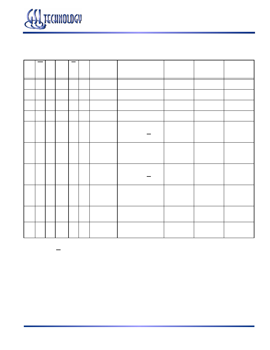
Double Late Write, Pipelined Read Truth Table
CK
E1
(tn)
E
(tn)
ADV
(tn)
W
(tn)
B
(tn)
Previous
Operation
Current Operation
DQ/CQ
(tn)
DQ/CQ
(tn+1)
DQ/CQ
(tn+2)
0→1
X
F
0
X
Bank Deselect
***/***
Hi-Z/Hi-Z
---
0→1
X
1
X
Bank Deselect Bank Deselect (Continue)
Hi-Z/Hi-Z
---
0→1
1
T
0
X
Deselect
***/***
Hi-Z/CQ
---
0→1
X
1
X
Deselect
Deselect (Continue)
Hi-Z/CQ
---
0→1
0
T
0
T
X
Write
Loads new address
Stores DQx if Bx = 0
***/***
D1/CQ
0→1
0
T
0
F
X
Write (Abort)
Loads new address
No data stored
***/***
Hi-Z/CQ
0→1
X
1
X
T
Write
Write Continue
Increments address by 1
Stores DQx if Bx = 0
***/***
Dn-1/CQ
Dn/CQ
0→1
X
1
X
F
Write
Write Continue (Abort)
Increments address by 1
No data stored
***/***
Dn-1/CQ
Hi-Z/CQ
0→1
0
T
0
1
X
Read
Loads new address
***/***
Q1/CQ
---
0→1
X
1
X
Read
Read Continue
Increments address by 1
Qn-1/CQ
Qn/CQ
---
Notes:
1. If E2 = EP2 and E3 = EP3, then E = “T” else E = “F”.
2. If one or more Bx = 0, then B = “T” else B = “F”.
3. “1” = input “high”; “0” = input “l(fā)ow”; “X” = input “don’t care”; “T” = input “true”; “F” = input “false”.
4. “***” indicates that the DQ input requirement / output state and CQ output state are determined by the previous operation.
5.
“---” indicates that the DQ input requirement / output state and CQ output state are determined by the next operation.
6. DQs are tristated in response to Bank Deselect, Deselect, and Write commands, one full cycle after the command is sampled.
7. CQs are tristated in response to Bank Deselect commands only, one full cycle after the command is sampled.
8. Up to three (3) Continue operations may be initiated after a Read or Write operation is initiated to burst transfer up to four (4) distinct pieces
of data per single external address input. If a fourth (4th) Continue operation is initiated, the internal address wraps back to the initial exter-
nal (base) address.
相關(guān)PDF資料 |
PDF描述 |
|---|---|
| GS8171DW72AGC-350IT | 256K X 72 STANDARD SRAM, 1.7 ns, PBGA209 |
| GS820H32GT-138I | 64K X 32 CACHE SRAM, 9.7 ns, PQFP100 |
| GS820H32GT-5I | 64K X 32 CACHE SRAM, 12 ns, PQFP100 |
| GS832032AGT-200 | CACHE SRAM, PQFP100 |
| GS8320V32GT-166IT | 1M X 32 CACHE SRAM, 8 ns, PQFP100 |
相關(guān)代理商/技術(shù)參數(shù) |
參數(shù)描述 |
|---|---|
| GS8171DW72AGC-300 | 制造商:GSI Technology 功能描述:SRAM SYNC OCTAL 1.8V 18MBIT 256KX72 1.8NS 209FBGA - Trays |
| GS8171DW72AGC-333 | 制造商:GSI Technology 功能描述:SRAM SYNC OCTAL 1.8V 18MBIT 256KX72 1.8NS 209FBGA - Trays |
| GS8171DW72AGC-350 | 制造商:GSI Technology 功能描述:SRAM SYNC OCTAL 1.8V 18MBIT 256KX72 1.7NS 209FBGA - Trays |
| GS8171DW72AGC-350I | 制造商:GSI Technology 功能描述:SRAM SYNC OCTAL 1.8V 18MBIT 256KX72 1.7NS 209FBGA - Trays |
| GS8180Q36D-167X | 制造商:GSI Technology 功能描述:512K X 36 (18 MEG)SIGMA QUAD I -SEPERATE I/O BURST OF 2 - Trays |
發(fā)布緊急采購,3分鐘左右您將得到回復(fù)。