- 您現(xiàn)在的位置:買賣IC網(wǎng) > PDF目錄299161 > GS8171DW72AGC-350IT (GSI TECHNOLOGY) 256K X 72 STANDARD SRAM, 1.7 ns, PBGA209 PDF資料下載
參數(shù)資料
| 型號(hào): | GS8171DW72AGC-350IT |
| 廠商: | GSI TECHNOLOGY |
| 元件分類: | SRAM |
| 英文描述: | 256K X 72 STANDARD SRAM, 1.7 ns, PBGA209 |
| 封裝: | 14 X 22 MM, 1 MM PITCH, LEAD FREE, BGA-209 |
| 文件頁數(shù): | 16/33頁 |
| 文件大小: | 1041K |
| 代理商: | GS8171DW72AGC-350IT |
第1頁第2頁第3頁第4頁第5頁第6頁第7頁第8頁第9頁第10頁第11頁第12頁第13頁第14頁第15頁當(dāng)前第16頁第17頁第18頁第19頁第20頁第21頁第22頁第23頁第24頁第25頁第26頁第27頁第28頁第29頁第30頁第31頁第32頁第33頁
GS8171DW36/72AC-350/333/300/250
Specifications cited are subject to change without notice. For latest documentation see http://www.gsitechnology.com.
Rev: 1.04 4/2005
23/33
2003, GSI Technology
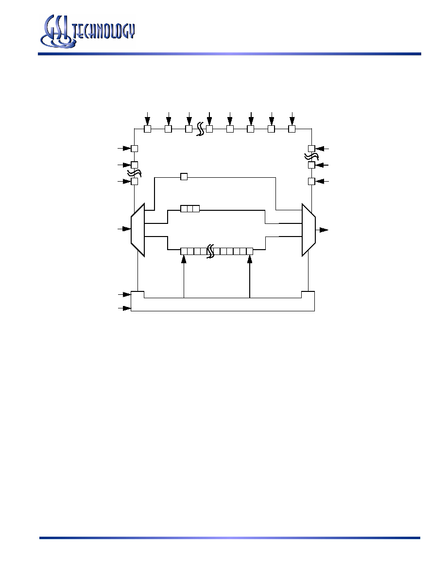
JTAG TAP Block Diagram
Identification (ID) Register
The ID Register is a 32-bit register that is loaded with a device and vendor specific 32-bit code when the controller is put in
Capture-DR state with the IDCODE command loaded in the Instruction Register. The code is loaded from a 32-bit on-chip ROM.
It describes various attributes of the RAM as indicated below. The register is then placed between the TDI and TDO pins when the
controller is moved into Shift-DR state. Bit 0 in the register is the LSB and the first to reach TDO when shifting begins.
Instruction Register
ID Code Register
Boundary Scan Register
0
1
2
0
31 30 29
1
2
0
Bypass Register
TDI
TDO
TMS
TCK
Test Access Port (TAP) Controller
108
1
0
Control Signals
相關(guān)PDF資料 |
PDF描述 |
|---|---|
| GS820H32GT-138I | 64K X 32 CACHE SRAM, 9.7 ns, PQFP100 |
| GS820H32GT-5I | 64K X 32 CACHE SRAM, 12 ns, PQFP100 |
| GS832032AGT-200 | CACHE SRAM, PQFP100 |
| GS8320V32GT-166IT | 1M X 32 CACHE SRAM, 8 ns, PQFP100 |
| GS832236B-225 | 1M X 36 CACHE SRAM, 7 ns, PBGA119 |
相關(guān)代理商/技術(shù)參數(shù) |
參數(shù)描述 |
|---|---|
| GS8180Q36D-167X | 制造商:GSI Technology 功能描述:512K X 36 (18 MEG)SIGMA QUAD I -SEPERATE I/O BURST OF 2 - Trays |
| GS8180QV36BGD-167 | 制造商:GSI Technology 功能描述:SRAM SYNC DUAL 2.5V 18MBIT 512KX36 2.5NS 165FPBGA - Trays |
| GS8180QV36BGD-167I | 制造商:GSI Technology 功能描述:SRAM SYNC DUAL 2.5V 18MBIT 512KX36 2.5NS 165FPBGA - Trays |
| GS8182D08BD-167 | 制造商:GSI Technology 功能描述:SRAM SYNC DUAL 1.8V 16MBIT 2MX8 0.5NS 165FPBGA - Trays |
| GS8182D08BD-250 | 制造商:GSI Technology 功能描述:SRAM SYNC DUAL 1.8V 16MBIT 2MX8 0.45NS 165FPBGA - Trays |
發(fā)布緊急采購,3分鐘左右您將得到回復(fù)。