- 您現(xiàn)在的位置:買賣IC網(wǎng) > PDF目錄299161 > GS8324Z72GC-133IT (GSI TECHNOLOGY) 512K X 72 ZBT SRAM, 10 ns, PBGA209 PDF資料下載
參數(shù)資料
| 型號: | GS8324Z72GC-133IT |
| 廠商: | GSI TECHNOLOGY |
| 元件分類: | SRAM |
| 英文描述: | 512K X 72 ZBT SRAM, 10 ns, PBGA209 |
| 封裝: | 14 X 22 MM, 1 MM PITCH, BGA-209 |
| 文件頁數(shù): | 46/46頁 |
| 文件大?。?/td> | 1157K |
| 代理商: | GS8324Z72GC-133IT |
第1頁第2頁第3頁第4頁第5頁第6頁第7頁第8頁第9頁第10頁第11頁第12頁第13頁第14頁第15頁第16頁第17頁第18頁第19頁第20頁第21頁第22頁第23頁第24頁第25頁第26頁第27頁第28頁第29頁第30頁第31頁第32頁第33頁第34頁第35頁第36頁第37頁第38頁第39頁第40頁第41頁第42頁第43頁第44頁第45頁當前第46頁
Rev: 1.00 10/2001
9/46
2001, Giga Semiconductor, Inc.
Specifications cited are subject to change without notice. For latest documentation see http://www.gsitechnology.com.
Preliminary
GS8324Z18(B/C)/GS8324Z36(B/C)/GS8324Z72(C)
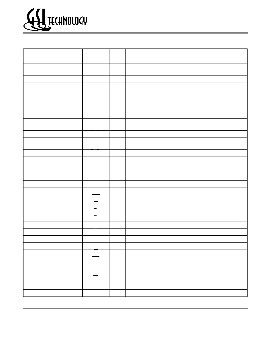
GS8324Z18/36 119-Bump BGA Pin Description
Pin Location
Symbol
Type
Description
P4, N4
A0, A1
I
Address field LSBs and Address Counter Preset Inputs
R2, C3, B3, C2, A2, A3, A5, A6, T3,
T5, R6, C5, B5, C6, G4, A4
An
I
Address Inputs
T4, T6
An
Address Input (x36 Version)
T2
NC
—
No Connect (x36 Version)
T2, T6, T4
An
I
Address Input (x18 Version)
K7, L7, N7, P7, K6, L6, M6, N6
H7, G7, E7, D7, H6, G6, F6, E6
H1, G1, E1, D1, H2, G2, F2, E2
K1, L1, N1, P1, K2, L2, M2, N2
DQA1–DQA8
DQB1–DQB8
DQC1–DQC8
DQD1–DQD8
I/O
Data Input and Output pins. (x36 Version)
P6, D6, D2, P2
DQA9, DQB9,
DQC9, DQD9
I/O
Data Input and Output pins. (x36 Version)
L5, G5, G3, L3
BA, BB, BC, BD
I
Byte Write Enable for DQA, DQB, DQC, DQD I/Os; active low (x36 Version)
P7, N6, L6, K7, H6, G7, F6, E7, D6
D1, E2, G2, H1, K2, L1, M2, N1, P2
DQA1–DQA9
DQB1–DQB9
I/O
Data Input and Output pins (x18 Version)
L5, G3
BA, BB
I
Byte Write Enable for DQA, DQB I/Os; active low (x18 Version)
B1, C1, R1, T1, U6, B7, C7, J3, J5
NC
—
No Connect
P6, N7, M6, L7, K6, H7, G6, E6, D7,
D2, E1, F2, G1, H2, K1, L2, N2, P1,
G5, L3
NC
—
No Connect (x18 Version)
L4
NC
—
No Connect (x36 Version)
K4
CK
I
Clock Input Signal; active high
M4
CKE
I
Clock Enable; active low
H4
W
I
Write Enable; active low
E4
E1
I
Chip Enable; active low
B6
E3
I
Chip Enable; active low (x36 version)
B2
E2
I
Chip Enable; active high (x36 version)
F4
G
I
Output Enable; active low
B4
ADV
I
Burst address counter advance enable
T7
ZZ
I
Sleep mode control; active high
R5
FT
I
Flow Through or Pipeline mode; active low
R3
LBO
I
Linear Burst Order mode; active low
D4
ZQ
I
FLXDrive Output Impedance Control (Low = Low Impedance [High Drive],
High = High Impedance [Low Drive])
R7
PE
I
Parity Bit Enable; active low
U2
TMS
I
Scan Test Mode Select
U3
TDI
I
Scan Test Data In
相關PDF資料 |
PDF描述 |
|---|---|
| GS840E18GB-100T | 256K X 18 CACHE SRAM, 12 ns, PBGA119 |
| GS840E18GB-180 | 256K X 18 CACHE SRAM, 8 ns, PBGA119 |
| GS8641E18F-200IT | 4M X 18 CACHE SRAM, 7.5 ns, PBGA165 |
| GS8641Z18GF-167T | 4M X 18 ZBT SRAM, 8 ns, PBGA165 |
| GS8642V18E-250 | 4M X 18 CACHE SRAM, 6.5 ns, PBGA165 |
相關代理商/技術參數(shù) |
參數(shù)描述 |
|---|---|
| GS8342D06BD-350 | 制造商:GSI Technology 功能描述:165 FBGA - Bulk |
| GS8342D06BD-500 | 制造商:GSI Technology 功能描述:165 FBGA - Bulk |
| GS8342D06BD-550 | 制造商:GSI Technology 功能描述:165 FBGA - Bulk |
| GS8342D06BD-550I | 制造商:GSI Technology 功能描述:165 FBGA - Bulk |
| GS8342D08AE-167 | 制造商:GSI Technology 功能描述:SRAM SYNC DUAL 1.8V 36MBIT 4MX8 0.5NS 165FPBGA - Trays |
發(fā)布緊急采購,3分鐘左右您將得到回復。