- 您現(xiàn)在的位置:買賣IC網(wǎng) > PDF目錄370472 > HD66841 (Hitachi,Ltd.) LVIC-II (LCD Video Interface Controller)(LCD視頻控制器) PDF資料下載
參數(shù)資料
| 型號(hào): | HD66841 |
| 廠商: | Hitachi,Ltd. |
| 英文描述: | LVIC-II (LCD Video Interface Controller)(LCD視頻控制器) |
| 中文描述: | LVIC - 2(液晶視頻接口控制器)(液晶顯示視頻控制器) |
| 文件頁數(shù): | 26/62頁 |
| 文件大小: | 185K |
| 代理商: | HD66841 |
第1頁第2頁第3頁第4頁第5頁第6頁第7頁第8頁第9頁第10頁第11頁第12頁第13頁第14頁第15頁第16頁第17頁第18頁第19頁第20頁第21頁第22頁第23頁第24頁第25頁當(dāng)前第26頁第27頁第28頁第29頁第30頁第31頁第32頁第33頁第34頁第35頁第36頁第37頁第38頁第39頁第40頁第41頁第42頁第43頁第44頁第45頁第46頁第47頁第48頁第49頁第50頁第51頁第52頁第53頁第54頁第55頁第56頁第57頁第58頁第59頁第60頁第61頁第62頁

HD66841
26
Dot Clock Generation
The dot clock, which is a data latch clock, is not a standard video signal, so it is not usually output from the
CRT display plug. Therefore, the HD66841 must generate it. The HD66841 has a programmable counter
and a phase comparator which are parts of a phase-locked loop (PLL) circuit, and it can generate the dot
clock from the HSYNC signal if a charge pump, a low-pass filter (LPF), and a voltage-controlled oscillator
(VCO) are externally attached.
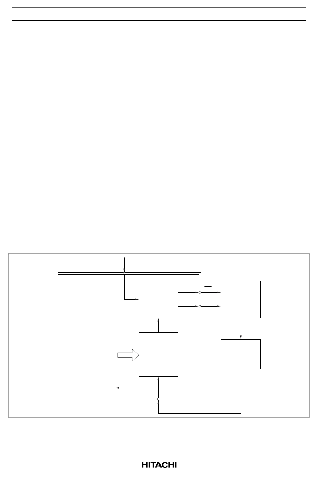
A block diagram of the PLL circuit is shown in Figure 11. A PLL circuit is a feedback controller that
generates a clock whose frequency and phase are the same as those of a basic clock. The basic clock is the
HSYNC signal in this case.
At power-on, the VCO outputs to the programmable counter a signal whose frequency is determined by the
voltage at the time. The counter divides the frequency of the signal according to the value in the PLL
frequency-dividing ratio register (R10, R11) and outputs it to the phase comparator. This is the frequency-
divided clock.
The comparator compares the edges of the clock pulses and the HSYNC signal pulses and output the
CU
or
CD
signal to the charge pump and LPF according to the result. The comparator outputs the
CU
signal if the
frequency of the clock is lower than that of the HSYNC signal or if the phase of the clock is behind that of
the HSYNC, signal; otherwise it outputs the
CD
signal. The charge pump and LPF apply a voltage to the
VCO according to the
CU
or
CD
signal.
This operation is repeated until the phase and frequency of the frequency-divided clock match those of the
HSYNC signal, making it a stable dot clock.
HSYNC
Phase
comparator
Frequency-
divided clock
Programmable
counter
DOTCLK
Timing clock generator
Written value in PLL
frequency-dividing ratio
register (R10, R11)
Inside HD66841
Charge pump
LPF
VCO
CU
CD
Figure 11 PLL Circuit Block Diagram
相關(guān)PDF資料 |
PDF描述 |
|---|---|
| HD68000Y-10 | MPU(MICRO PROCESSING UNIT) |
| HD68HC000Y-10 | MPU(MICRO PROCESSING UNIT) |
| HD68000Y-12 | MPU(MICRO PROCESSING UNIT) |
| HD68HC000Y-12 | MPU(MICRO PROCESSING UNIT) |
| HD68000Y-8 | MPU(MICRO PROCESSING UNIT) |
相關(guān)代理商/技術(shù)參數(shù) |
參數(shù)描述 |
|---|---|
| HD66841FP | 制造商:未知廠家 制造商全稱:未知廠家 功能描述:LCD Controller |
| HD66841FS | 制造商:未知廠家 制造商全稱:未知廠家 功能描述:LCD Controller |
| HD66850FP | 制造商:未知廠家 制造商全稱:未知廠家 功能描述:LCD Controller |
| HD6788 | 制造商:Coilcraft Inc 功能描述:DSL transformer, for Brooktree BT8921, not RoHS |
| HD6789 | 制造商:Coilcraft Inc 功能描述:DSL transformer, for Brooktree BT8921, not RoHS |
發(fā)布緊急采購,3分鐘左右您將得到回復(fù)。