- 您現(xiàn)在的位置:買賣IC網(wǎng) > PDF目錄371813 > HI3197 (HARRIS SEMICONDUCTOR) 10-Bit, 125 MSPS D/A Converter PDF資料下載
參數(shù)資料
| 型號(hào): | HI3197 |
| 廠商: | HARRIS SEMICONDUCTOR |
| 元件分類: | DAC |
| 英文描述: | 10-Bit, 125 MSPS D/A Converter |
| 中文描述: | PARALLEL, WORD INPUT LOADING, 0.0035 us SETTLING TIME, 10-BIT DAC, PQFP48 |
| 文件頁數(shù): | 17/25頁 |
| 文件大?。?/td> | 284K |
| 代理商: | HI3197 |
17
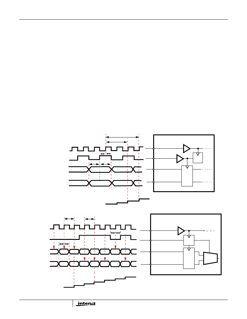
MUX.2 Mode
Set C1 and C3 Low and C2 High for this mode.
In MUX.2 mode, the clock is input to the clock input pin, and
the signal with a cycle half that of the clock (hereafter,
DlV2lN signal) is input to the DlV2IN pin at TTL level. The
DlV2lN signal is internally latched by the clock, so
consideration must be given to the setup time (t
S_DIV
) and
hold time (t
H_DIV
) with respect to the clock. In addition, the
data is loaded by the DlV2lN signal, so consideration must
also be given to the setup time (t
S
) and hold time (t
H
) with
respect to the DlV2IN signal. The data can be divided and
input to two systems: A (DA0 to DA9) and B (DB0 to DB9).
The data `is internally multiplexed, then the system A data is
output as an analog signal with a 2-clock pipeline delay, and
the system B data as an analog signal with a 3-clock pipeline
delay from the clock that loads the DIV2IN signal. See
Figure 9 for the detailed timing.
SELECT.A Mode and SELE.B Mode
Set C1 High and C2 and C3 Low for SELE.A mode.
In SELE.A mode, the clock is input to the clock input pin, and
the data is input to the system A (DA0 to DA9) data input pins.
Set C1 and C2 High and C3 Low for SELE.B mode.
In SELE.B mode, the clock is input to the clock input pin, and
the data is input to the system B (DB0 to DB9) data input
pins. In either mode, consideration must be given to the
setup time, (t
S
) and hold time (t
H
) with respect to the clock.
Also, the data is output as an analog signal with a 1-clock
pipeline delay after loading by the clock.
Switching between SELE.A mode and SELE.B mode is
done by switching the C2 pin between High and Low levels.
Also, the mode can be switched at high speed in sync with
the clock by inputting the switching signal (02 signal) to the
C2 pin. The C2 signal is internally latched by the clock, so
consideration must be given to the setup time (t
S_C2
) and
hold time (t
H_C2
) with respect to the clock. See Figure 10 for
the detailed timing.
FIGURE 9. MUX.2 MODE
FIGURE 10. SELECT A MODE AND SELECT B MODE
CXA3197 (MUX.2 MODE)
CLOCK INPUT PIN
DIV2IN INPUT
PIN
DA0 TO DA9
DB0 TO DB9
t
PD
(B)
t
PD
(A)
0
2
3
1
t
S_DIV
t
H_DIV
t
S
t
H
A0
A2
A1
A0
A1
B0
B1
B2
B1
B0
CLOCK
DIV2IN SIGNAL
SYSTEM A DATA
SYSTEM B DATA
ANALOG OUTPUT SIGNAL
CXA3197
CLOCK INPUT PIN
C2 INPUT
PIN
DA0 TO DA9
DB0 TO DB9
(SELE.A MODE/SELE.B MODE)
SELECT
t
PD
(A)
t
PD
(B)
0
0
1
1
t
A_C2
t
H_C2
t
S
t
H
A0
A1
A2
A6
A8
B3
B5
B7
B4
A0
A1
A2
B3
B4
B5
A6
CLOCK
C2 SIGNAL
SYSTEM A DATA
SYSTEM B DATA
ANALOG OUTPUT SIGNAL
HI3197
相關(guān)PDF資料 |
PDF描述 |
|---|---|
| HI3276JCQ | Small glass bead with axial leads |
| HI3338KIB | TVS 6.0V 300W UNI-DIR SOT-23 |
| HI3338KIP | TVS DUAL-UNI SGL-BI 300MW SOT-23 |
| HI3338 | 8-Bit, CMOS R2R D/A Converter |
| HI4P0222-5 | High Frequency/Video Switch |
相關(guān)代理商/技術(shù)參數(shù) |
參數(shù)描述 |
|---|---|
| HI3197JCQ | 制造商:Rochester Electronics LLC 功能描述:- Bulk |
| HI31C | 制造商:HSMC 制造商全稱:HSMC 功能描述:NPN EPITAXIAL PLANAR TRANSISTOR |
| HI-3200 | 制造商:HOLTIC 制造商全稱:Holt Integrated Circuits 功能描述:AVIONICS DATA MANAGEMENT ENGINE |
| HI-3200CQI | 制造商:HOLTIC 制造商全稱:Holt Integrated Circuits 功能描述:AVIONICS DATA MANAGEMENT ENGINE |
| HI-3200CQIF | 制造商:HOLTIC 制造商全稱:Holt Integrated Circuits 功能描述:AVIONICS DATA MANAGEMENT ENGINE |
發(fā)布緊急采購,3分鐘左右您將得到回復(fù)。