- 您現(xiàn)在的位置:買賣IC網(wǎng) > PDF目錄383075 > HSP50214AVC (HARRIS SEMICONDUCTOR) Programmable Downconverter PDF資料下載
參數(shù)資料
| 型號(hào): | HSP50214AVC |
| 廠商: | HARRIS SEMICONDUCTOR |
| 元件分類: | 通信及網(wǎng)絡(luò) |
| 英文描述: | Programmable Downconverter |
| 中文描述: | SPECIALTY TELECOM CIRCUIT, PQFP120 |
| 文件頁數(shù): | 38/60頁 |
| 文件大?。?/td> | 467K |
| 代理商: | HSP50214AVC |
第1頁第2頁第3頁第4頁第5頁第6頁第7頁第8頁第9頁第10頁第11頁第12頁第13頁第14頁第15頁第16頁第17頁第18頁第19頁第20頁第21頁第22頁第23頁第24頁第25頁第26頁第27頁第28頁第29頁第30頁第31頁第32頁第33頁第34頁第35頁第36頁第37頁當(dāng)前第38頁第39頁第40頁第41頁第42頁第43頁第44頁第45頁第46頁第47頁第48頁第49頁第50頁第51頁第52頁第53頁第54頁第55頁第56頁第57頁第58頁第59頁第60頁
38
NOTE: In the Status output, BOUT(7:0) are all GND.
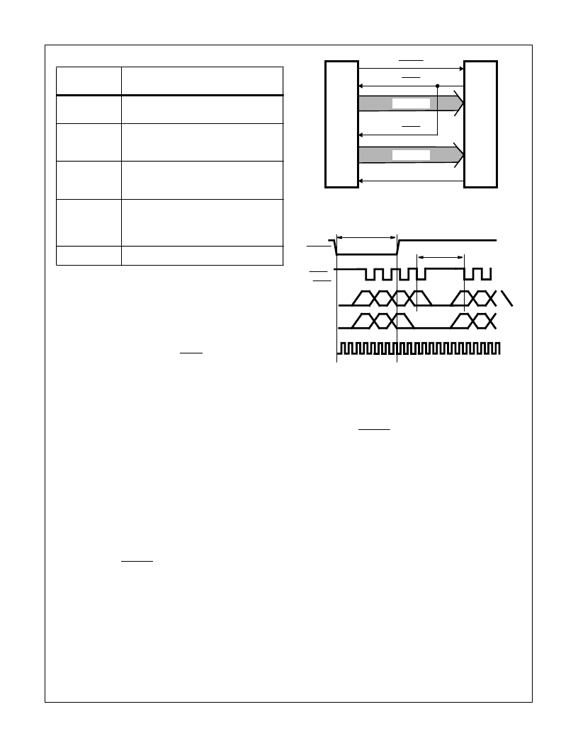
Figure 38 shows the interface between a 16-bit microproces-
sor (or other baseband processing engine) and the Buffer
RAM Output Section of the Programmable Down Converter,
configured for data output via the parallel outputs AOUT and
BOUT. In the 16-bit microprocessor interface configuration,
the Buffer RAM pointer is incremented when the
μ
Processor
reads address SEL(2:0) = 7 and OEBL = 0.
After reset, the FIFO must be incremented to read the first
sample set. This is because the RAM read and write pointers
cannot point to the same address. Thus, the FIFO pointer
must move to the next address before reading the next set of
data (I, Q, |r|,
φ
, and
f
) samples. 4 PROCCLK cycles are
required after an increment before reading can resume. The
FIFO write pointer is reset to zero (the first data sample) when
Control Word 22 is written to via the 8-bit microprocessor
interface. See the Microprocessor Read Section for more
detail on how to obtain the Buffer RAM output with this tech-
nique. Figure 36 shows the timing diagram required for paral-
lel output operations. In this diagram, only the I, Q and
Frequency data are taken from each sample before incre-
menting to the next sample. Figure 36 assumes that the
pointer has already been incremented into a sample.
NOTE: For the very first sample read, the pointer must be incre-
mented first and 4 PROCCLKs must pass before this
sample can be read.
Figure 39 shows INTRRP going low before the FIFO is read.
The FIFO can be read before the number of samples
reaches the INTRRP pointer. The number of samples in the
FIFO must be monitored by the user via a status read.
Suppose the depth of the Buffer RAM Output Section is pro-
grammed for an INTRRP pointer depth of 4. If the output is
at 4 times the baud rate, the processing routine for the
microprocessor may only need to read the buffer when the
Buffer RAM had 4 samples since processing is usually on a
baud by baud basis.
Figure 40 illustrates the conceptual view of the FIFO as a cir-
cular buffer, with the Write address one step ahead of the
Read Address.
Figure 40A deals with clockwise read and write address
incrementing. The FIFO depth is the difference between the
Write and Read pointers, modulo 8. Figure 40B illustrates a
FIFO status of Full, while Figure 40C illustrates a FIFO
empty status condition. Figure 40D illustrates a programmed
FIFO depth of 3 and the INTRRP signal indicating that the
buffer has sufficient data to be read.
Following some simple rules for operating the FIFO will elim-
inate most operational errors:
Rule #1: The Read and Write Pointers cannot point at the
same address (the circuitry will not allow this).
Rule #2: The FIFO is full when the Write Address = Read
Address -1 (no more data will be written until some samples
are read or the FIFO is reset).
TABLE 18. STATUS BIT DEFINITIONS
AOUT BIT
LOCATION
INFORMATION
(7:5)
FIFO depth - When in FIFO mode, these bits
are the current depth of the FIFO.
4
EMPTY - When in FIFO mode, the FIFO is
empty, and the read pointer cannot be ad-
vanced. Active High.
3
FULL - When in FIFO mode, the FIFO is full,
and new samples will not be written.
Active High.
2
READYB - When in FIFO mode, the output buff-
er has reached the programmed threshold. In
the snapshot mode, the programmed number
of samples have been taken. Active Low.
1-0
GND
H
INTRRP
OEAL
OEBL
PDC
16-BIT
μ
P
SEL(2:0)
BOUT(7:0)
AOUT(7:0)
FIGURE 38. INTERFACE BETWEEN A 16-BIT MICROPROCES-
SOR AND PDC IN FIFO BUFFER RAM MODE
INT
RD
D(15:8)
D(7:0)
A(2:0)
1
2 3 4
1 2 3 4
5 6 7 8
0
1
4
7
0
1
INTRRP
OEAL,
OEBL
SEL(0:2)
I
Q
FR
I
Q
AOUT(7:0),
BOUT(7:0)
PROCCLK
8 CLKS
> 4 CLKS
FIGURE 39. TIMING DIAGRAM FOR PDC IN FIFO MODE WITH
OUTPUTS I, Q, AND FREQUENCY SENT TO
AOUT(7:0) AND BOUT(7:0)
HSP50214A
相關(guān)PDF資料 |
PDF描述 |
|---|---|
| HSP50214AVI | Programmable Downconverter |
| HSP50214B | Programmable Downconverter |
| HSP50214BVC | Programmable Downconverter |
| HSP50214BVI | Programmable Downconverter |
| HT84 | ADSL Coupling Transformers |
相關(guān)代理商/技術(shù)參數(shù) |
參數(shù)描述 |
|---|---|
| HSP50214AVI | 制造商:INTERSIL 制造商全稱:Intersil Corporation 功能描述:Programmable Downconverter |
| HSP50214B | 制造商:INTERSIL 制造商全稱:Intersil Corporation 功能描述:Programmable Downconverter |
| HSP50214B_07 | 制造商:INTERSIL 制造商全稱:Intersil Corporation 功能描述:Programmable Downconverter |
| HSP50214BVC | 功能描述:上下轉(zhuǎn)換器 120L MQFP COMTEMP 14-BIT PROGRAMMABLE DOWNCONVERTER 65MSPS RoHS:否 制造商:Texas Instruments 產(chǎn)品:Down Converters 射頻:52 MHz to 78 MHz 中頻:300 MHz LO頻率: 功率增益: P1dB: 工作電源電壓:1.8 V, 3.3 V 工作電源電流:120 mA 最大功率耗散:1 W 最大工作溫度:+ 85 C 安裝風(fēng)格:SMD/SMT 封裝 / 箱體:PQFP-128 |
| HSP50214BVCZ | 功能描述:上下轉(zhuǎn)換器 120L MQFP COMTEMP 14-BIT PROG DWNCNVRT RoHS:否 制造商:Texas Instruments 產(chǎn)品:Down Converters 射頻:52 MHz to 78 MHz 中頻:300 MHz LO頻率: 功率增益: P1dB: 工作電源電壓:1.8 V, 3.3 V 工作電源電流:120 mA 最大功率耗散:1 W 最大工作溫度:+ 85 C 安裝風(fēng)格:SMD/SMT 封裝 / 箱體:PQFP-128 |
發(fā)布緊急采購(gòu),3分鐘左右您將得到回復(fù)。