- 您現(xiàn)在的位置:買賣IC網(wǎng) > PDF目錄296198 > HYB25D128400CT-5 (QIMONDA AG) 32M X 4 DDR DRAM, 0.7 ns, PDSO66 PDF資料下載
參數(shù)資料
| 型號: | HYB25D128400CT-5 |
| 廠商: | QIMONDA AG |
| 元件分類: | DRAM |
| 英文描述: | 32M X 4 DDR DRAM, 0.7 ns, PDSO66 |
| 封裝: | PLASTIC, TSOP2-66 |
| 文件頁數(shù): | 21/44頁 |
| 文件大小: | 2618K |
| 代理商: | HYB25D128400CT-5 |
第1頁第2頁第3頁第4頁第5頁第6頁第7頁第8頁第9頁第10頁第11頁第12頁第13頁第14頁第15頁第16頁第17頁第18頁第19頁第20頁當前第21頁第22頁第23頁第24頁第25頁第26頁第27頁第28頁第29頁第30頁第31頁第32頁第33頁第34頁第35頁第36頁第37頁第38頁第39頁第40頁第41頁第42頁第43頁第44頁
HYB25D128[40/80/16]0C[C/E/F/T]
128-Mbit Double-Data-Rate SDRAM
Internet Data Sheet
Rev. 1.70, 2008-04
28
03292006-U5AN-6TI1
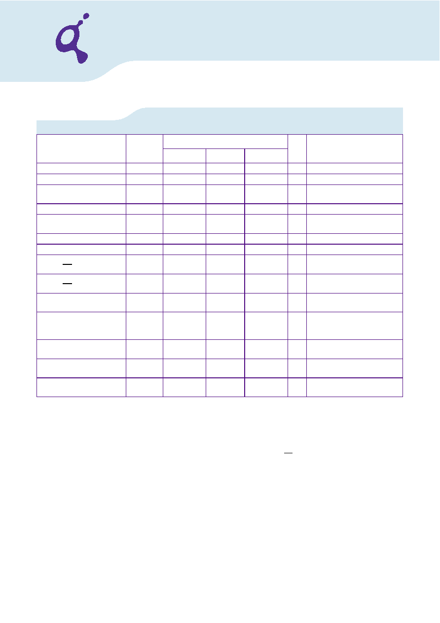
TABLE 21
Electrical Characteristics and DC Operating Conditions
1) 0
°C ≤ T
A ≤ 70 °C; VDD = VDDQ = 2.5 V ± 0.2 V
2) Under all conditions,
V
DDQ must be less than or equal to VDD.
3) Peak to peak AC noise on
V
REF may not exceed ± 2% VREF.DC. VREF is also expected to track noise variations in VDDQ.
4)
V
TT is not applied directly to the device. VTT is a system supply for signal termination resistors, is expected to be set equal to VREF, and
must track variations in the DC level of
V
REF.
5) Inputs are not recognized as valid until
V
REF stabilizes.
6)
V
ID is the magnitude of the difference between the input level on CK and the input level on CK.
7) The ratio of the pull-up current to the pull-down current is specified for the same temperature and voltage, over the entire temperature and
voltage range, for device drain to source voltage from 0.25 to 1.0 V. For a given output, it represents the maximum difference between
pull-up and pull-down drivers due to process variation.
8) Values are shown per pin.
Parameter
Symbol
Values
Unit Note/Test Condition 1)
Min.
Typ.
Max.
Device Supply Voltage
V
DD
2.3
2.5
2.7
V
f
CK ≤ 200 MHz
Output Supply Voltage
V
DDQ
2.3
2.5
2.7
V
f
CK ≤ 200 MHz
Supply Voltage,
I/O Supply Voltage
V
SS, VSSQ
00
V
—
Input Reference Voltage
V
REF
0.49
× V
DDQ
0.5
× V
DDQ
0.51
× V
DDQ
V
I/O Termination Voltage
(System)
V
TT
V
REF – 0.04
V
REF + 0.04
V
Input High (Logic1) Voltage
V
IH.DC
V
REF + 0.15
V
DDQ + 0.3
V
Input Low (Logic0) Voltage
V
IL.DC
–0.3
V
REF – 0.15
V
Input Voltage Level,
CK and CK Inputs
V
IN.DC
–0.3
V
DDQ + 0.3
V
Input Differential Voltage,
CK and CK Inputs
V
ID.DC
0.36
VDDQ + 0.6
V
VI-Matching Pull-up Current
to Pull-down Current
VI
Ratio
0.71
1.4
—
Input Leakage Current
I
I
–2
2
μA
Any input 0 V
≤ V
IN ≤ VDD;
All other pins not under test
=0V 8)
Output Leakage Current
I
OZ
–5
5
μA
DQs are disabled;
0V
≤ V
OUT ≤ VDDQ
Output High Current,
Normal Strength Driver
I
OH
—
–16.2
mA
V
OUT = 1.95 V
Output Low Current,
Normal Strength Driver
I
OL
–16.2
—
mA
V
OUT = 0.35 V
相關PDF資料 |
PDF描述 |
|---|---|
| HYB25D256160CC-5 | 256 Mbit Double Data Rate SDRAM |
| HYB25S256160AC-7.5 | 16M X 16 SYNCHRONOUS DRAM, 7.5 ns, PBGA54 |
| HYB39S128160TEL-37 | MEMORY SPECTRUM |
| HYB39S128160TEL-5 | MEMORY SPECTRUM |
| HYB39S128160TEL-7 | MEMORY SPECTRUM |
相關代理商/技術參數(shù) |
參數(shù)描述 |
|---|---|
| HYB25D128400CT-7 | 制造商:INFINEON 制造商全稱:Infineon Technologies AG 功能描述:128 Mbit Double Data Rate SDRAM |
| HYB25D128800AT-6 | 制造商:INFINEON 制造商全稱:Infineon Technologies AG 功能描述:128 Mbit Double Data Rate SDRAM |
| HYB25D128800AT-7 | 制造商:INFINEON 制造商全稱:Infineon Technologies AG 功能描述:128 Mbit Double Data Rate SDRAM |
| HYB25D128800AT-8 | 制造商:未知廠家 制造商全稱:未知廠家 功能描述:?128Mb (16Mx8) DDR200 (2-2-2)? |
| HYB25D128800ATL-6 | 制造商:INFINEON 制造商全稱:Infineon Technologies AG 功能描述:128 Mbit Double Data Rate SDRAM |
發(fā)布緊急采購,3分鐘左右您將得到回復。