- 您現(xiàn)在的位置:買(mǎi)賣(mài)IC網(wǎng) > PDF目錄370794 > HYE18P32160AC-125 (INFINEON TECHNOLOGIES AG) M39012 MIL RF CONNECTOR PDF資料下載
參數(shù)資料
| 型號(hào): | HYE18P32160AC-125 |
| 廠(chǎng)商: | INFINEON TECHNOLOGIES AG |
| 英文描述: | M39012 MIL RF CONNECTOR |
| 中文描述: | 32M的同步突發(fā)的CellularRAM |
| 文件頁(yè)數(shù): | 14/53頁(yè) |
| 文件大?。?/td> | 1426K |
| 代理商: | HYE18P32160AC-125 |
第1頁(yè)第2頁(yè)第3頁(yè)第4頁(yè)第5頁(yè)第6頁(yè)第7頁(yè)第8頁(yè)第9頁(yè)第10頁(yè)第11頁(yè)第12頁(yè)第13頁(yè)當(dāng)前第14頁(yè)第15頁(yè)第16頁(yè)第17頁(yè)第18頁(yè)第19頁(yè)第20頁(yè)第21頁(yè)第22頁(yè)第23頁(yè)第24頁(yè)第25頁(yè)第26頁(yè)第27頁(yè)第28頁(yè)第29頁(yè)第30頁(yè)第31頁(yè)第32頁(yè)第33頁(yè)第34頁(yè)第35頁(yè)第36頁(yè)第37頁(yè)第38頁(yè)第39頁(yè)第40頁(yè)第41頁(yè)第42頁(yè)第43頁(yè)第44頁(yè)第45頁(yè)第46頁(yè)第47頁(yè)第48頁(yè)第49頁(yè)第50頁(yè)第51頁(yè)第52頁(yè)第53頁(yè)

HYE18P32160AC(-/L)9.6/12.5/15
32M Synchronous Burst CellularRAM
Overview
Data Sheet
14
V2.0, 2003-12-16
1.6.2
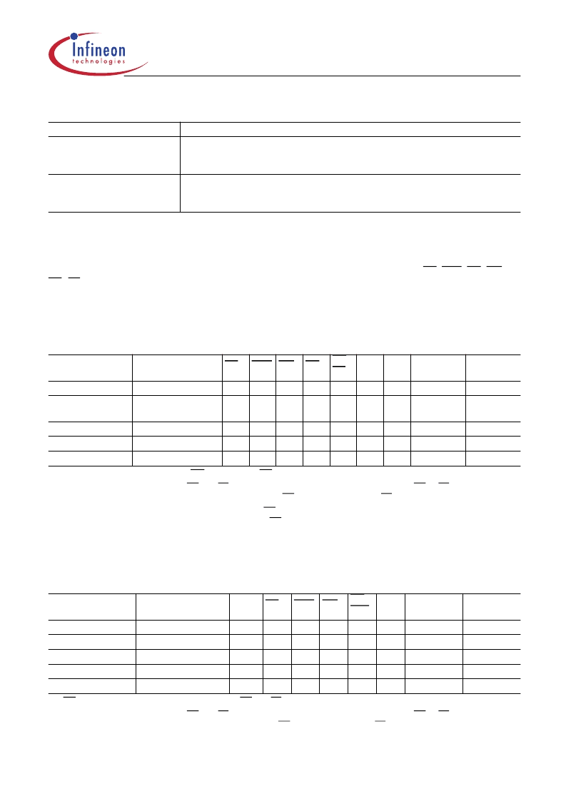
In NOR-Flash-type mode read commands are performed on a synchronous base whereas write commands are
performed in an asynchronous way.
In synchronous read mode all operations are defined by the states of the control signals CS, ADV, OE, WE and
UB, LB at the positive (default) edge of the data clock. To put the device in NOR-Flash-type mode the Bus
Configuration Register must be programmed first accordingly.
Table 5
lists the truth table for the supported asynchronous write commands, while
Table 5
lists the supported
synchronous read commands.
Commands Supported in NOR-Flash-Type Mode
Note:‘L’ represents a low voltage level, ‘H’ a high voltage level, ‘X’ represents “Don’t Care”, ‘V’ represents “Valid”.
DESELECT
The DESELECT function prevents new commands from being executed by the
CellularRAM. The CellularRAM is effectively deselected. I/O signals are put to
high impedance state.
DPD stops all refresh-related activities and entire on-chip circuit operation.
Current consumption drops below 25
μ
A. Wake-up from DPD also requires
150
μ
s to get ready for normal operation.
DPD
Table 5
Asynchronous Command Table (NOR-Flash-Type Mode)
Operation Mode
Power Mode
CS
ADV WE
OE
UB/
LB
L
2)
X
CRE A19
A20 - A0
DQ15:0
WRITE
SET CONTROL
REGISTER
NO OPERATION
DESELECT
DPD
4)
Active
Active
L
L
L
L
L
L
X
1)
X
1)
1) During a write access invoked by WE set to low the OE signal is ignored.
2)
Table 5
reflects the behaviour if UB and LB are asserted to low. If only either of the signals, UB or LB, is asserted to low
only the corresponding data byte will be output or written (UB enables DQ15 - DQ8, LB enables DQ7 - DQ0).
3) Stand-by power mode applies only to the case when CS goes low from DESELECT while no address change occurs. NO
OPERATION from any active power mode by keeping CS low consumes the power higher than stand-by mode.
4) Deep power down is maintained until control register is re-programmed to disable the bit for deep power down (RCR Bit 4).
L
H
V
L
H
X
X
X
ADR
RCR DIN
BCR DIN
X
X
X
DIN
X
Standby~Active
3)
Standby
Deep Power Down
L
H
H
H
X
X
H
X
X
H
X
X
X
X
X
L
L
X
High-Z
High-Z
High-Z
Table 6
Synchronous Command Table (NOR-Flash-Type Mode)
Operation Mode
Power Mode
CLK
CS
ADV WE
UB/
LB
1)
X
L
2)
X
X
X
1) OE does the same function to all DQ pins with UB and LB during read operation.
2)
Table 6
reflects the behaviour if UB and LB are asserted to low. If only either of the signals, UB or LB, is asserted to low
only the corresponding data byte will be output or written (UB enables DQ15 - DQ8, LB enables DQ7 - DQ0). If both signals
are disabled the device is put in deselect mode.
CRE
A20 - A0
DQ15:0
BURST INIT
BURST READ
NO OPERATION
DESELECT
DPD
6)
Active
Active
Standby~Active
4)
Standby
Deep Power Down
L->H
L->H
L->H
L->H
L
L
L
L
H
H
L
H
H
X
X
H
H
H
X
X
L
L
L
X
X
ADR
X
X
X
X
X
DOUT
3)
High-Z
5)
High-Z
High-Z
Table 4
Mode
Description of Commands (SRAM-Type Mode)
(cont’d)
Description
相關(guān)PDF資料 |
PDF描述 |
|---|---|
| HYE18P32160AC-15 | M39012 MIL RF CONNECTOR |
| HYE18P32161AC-85 | 32M Asynchronous/Page CellularRAM |
| HYE18P32161AC | 32M Asynchronous/Page CellularRAM |
| HYE18P32161ACL70 | JT 23C 21#20 2#16 SKT PLUG |
| HYE18P32161ACL85 | Circular Connector; MIL SPEC:MIL-DTL-38999 Series II; Body Material:Metal; Series:JT; No. of Contacts:11; Connector Shell Size:18; Connecting Termination:Crimp; Circular Shell Style:Straight Plug; Body Style:Straight RoHS Compliant: No |
相關(guān)代理商/技術(shù)參數(shù) |
參數(shù)描述 |
|---|---|
| HYE18P32160AC-15 | 制造商:INFINEON 制造商全稱(chēng):Infineon Technologies AG 功能描述:32M Synchronous Burst CellularRAM |
| HYE18P32160AC-96 | 制造商:INFINEON 制造商全稱(chēng):Infineon Technologies AG 功能描述:32M Synchronous Burst CellularRAM |
| HYE18P32160ACL125 | 制造商:INFINEON 制造商全稱(chēng):Infineon Technologies AG 功能描述:32M Synchronous Burst CellularRAM |
| HYE18P32160ACL15 | 制造商:INFINEON 制造商全稱(chēng):Infineon Technologies AG 功能描述:32M Synchronous Burst CellularRAM |
| HYE18P32160ACL96 | 制造商:INFINEON 制造商全稱(chēng):Infineon Technologies AG 功能描述:32M Synchronous Burst CellularRAM |
發(fā)布緊急采購(gòu),3分鐘左右您將得到回復(fù)。