- 您現(xiàn)在的位置:買賣IC網(wǎng) > PDF目錄360784 > ICS93701YGT DDR Phase Lock Loop Clock Driver PDF資料下載
參數(shù)資料
| 型號: | ICS93701YGT |
| 英文描述: | DDR Phase Lock Loop Clock Driver |
| 中文描述: | 復(fù)員鎖相環(huán)時鐘驅(qū)動器 |
| 文件頁數(shù): | 8/9頁 |
| 文件大小: | 184K |
| 代理商: | ICS93701YGT |
8
ICS93701
0417B—10/29/02
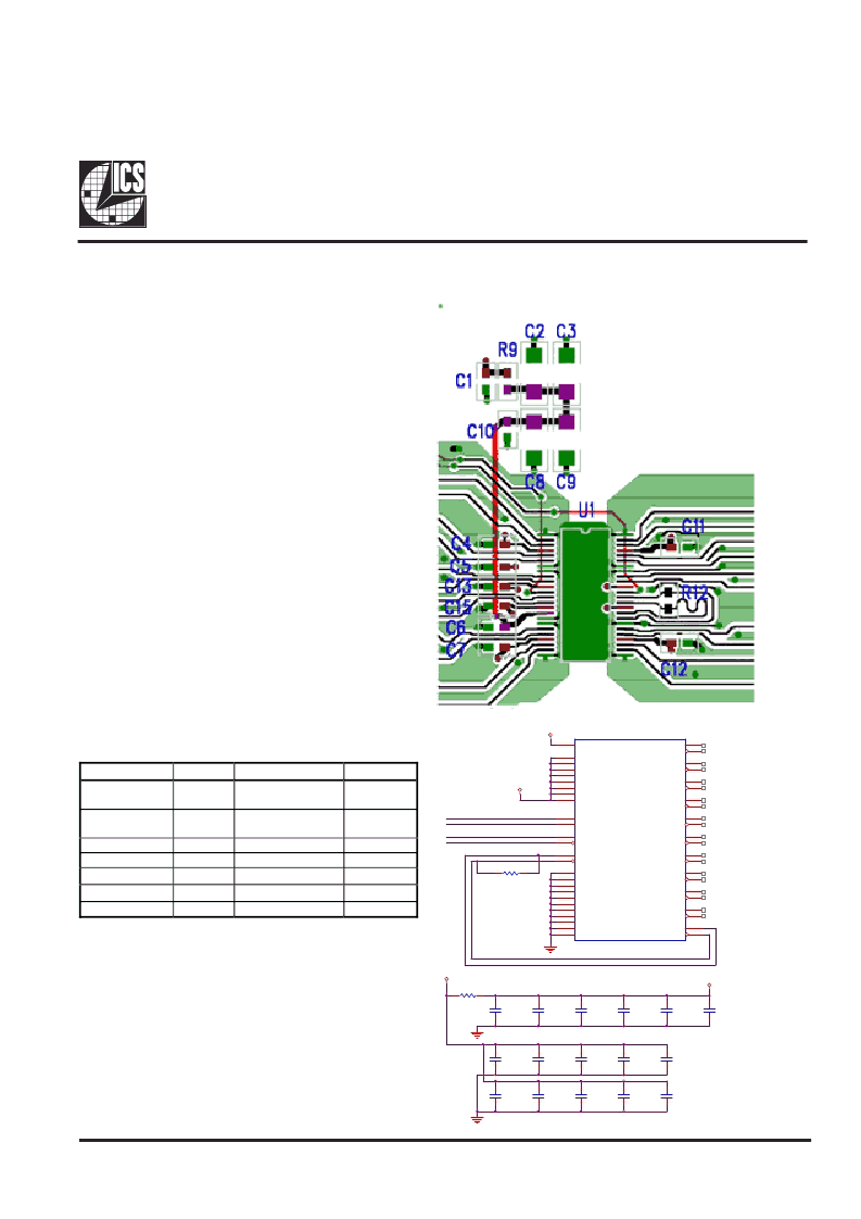
Recommended Layout for the ICS93701
General Layout Precautions:
Use copper flooded ground on the top signal layer under the
clock buffer The area under U1 on the right is an example.
Flood over the ground vias.
1) Use power vias for power and ground. Vias 20 mil or
larger in diameter have lower high frequency impedance.
Vias for signals may be minimum drill size.
2) Make all power and ground traces are as wide as the via
pad for lower inductance.
3) VAA for pin 16 has a low pass RC filter to decouple the
digital and analog supplies. The 4.7uF capacitors may be
replaced with a single low ESR device with the same
total capacitance. VAA is routed on a outside signal
layer. Do not cut a power or ground plane and route in it.
4) Notice that ground vias are never shared.
5) When ever possible, VCC (net V2P5 in the schematic)
pins have a decoupling capacitor. Power is always routed
from the plane connection via to the capacitor pad to the
VCC pin on the clock buffer. Moats or plane cuts are not
used to isolate power.
6) Differential mode clock output traces are routed:
a. With a ground trace between the pairs. Trace is
grounded on both ends.
b. Without a ground trace, clock pairs are routed with a
separation of at least 5 times the thickness of the
dielectric. If the dielectric thickness is 4.5 mil, the
trace separation is at least 18 mils.
Component Values:
Ref Desg.
Value
Description
C1,C4,C5,
C7,C11,C12
C2,C3,C8,
C9
C10
.22uF
CERAMIC MLC
C6
2200pF
CERAMIC MLC
R12
120
R9
4.7
U1
ICS93701AG
Package
0603
.01uF
CERAMIC MLC
4.7uF
CERAMIC MLC
1206
0603
0603
0603
0603
TSSOP48
C2
1
2
V2P5
FB_IN#
C3
1
2
V2A5
C9
1
2
C7
1
2
V2P5
C16
1
2
C10
1
2
C1
1
2
C5
1
2
C11
1
2
R12
120
1
2
V2A5
V2A5
CLK_IN#
U1
AVDD
ICS93701
16
4
11
15
21
28
34
38
45
1
7
8
18
24
25
31
41
42
48
17
35
36
13
14
37
12
3
2
5
6
10
9
20
19
22
23
46
47
44
43
39
40
29
30
27
26
33
32
VDD
VDD
VDD
VDD
VDD
VDD
VDD
VDD
GND
GND
GND
GND
FB_INT
FB_INC
CLK_INT
CLK_INC
SDA
SCL
CLKT0
CLKT1
CLKC1
CLKT2
CLKC2
CLKT3
CLKC3
CLKT4
CLKC4
CLKT5
CLKC5
CLKT6
CLKC6
CLKT7
CLKC7
CLKT8
CLKT9
FB_OUTT
C12
1
2
C6
1
2
SCL
SDA
R9
4.7
1
2
C13
1
2
C14
1
2
FB_IN
C8
1
2
C15
1
2
CLK_IN
C4
1
2
相關(guān)PDF資料 |
PDF描述 |
|---|---|
| ICS93705 | DDR Phase Lock Loop Zero Delay Clock Buffer |
| ICS93705YF-T | DDR Phase Lock Loop Zero Delay Clock Buffer |
| ICS93712YF-PPP-T | 2 DIMM DDR Fanout Buffer |
| ICS93712YF-T | 2 DIMM DDR Fanout Buffer |
| ICS93712 | 2 DIMM DDR Fanout Buffer |
相關(guān)代理商/技術(shù)參數(shù) |
參數(shù)描述 |
|---|---|
| ICS93705 | 制造商:ICS 制造商全稱:ICS 功能描述:DDR Phase Lock Loop Zero Delay Clock Buffer |
| ICS93705YF-T | 制造商:ICS 制造商全稱:ICS 功能描述:DDR Phase Lock Loop Zero Delay Clock Buffer |
| ICS93712 | 制造商:ICS 制造商全稱:ICS 功能描述:2 DIMM DDR Fanout Buffer |
| ICS93712YF-PPP-T | 制造商:ICS 制造商全稱:ICS 功能描述:2 DIMM DDR Fanout Buffer |
| ICS93712YF-T | 制造商:ICS 制造商全稱:ICS 功能描述:2 DIMM DDR Fanout Buffer |
發(fā)布緊急采購,3分鐘左右您將得到回復(fù)。