- 您現(xiàn)在的位置:買賣IC網(wǎng) > PDF目錄373086 > K9E2G08U0M-V (SAMSUNG SEMICONDUCTOR CO. LTD.) 256M x 8 Bits NAND Flash Memory PDF資料下載
參數(shù)資料
| 型號(hào): | K9E2G08U0M-V |
| 廠商: | SAMSUNG SEMICONDUCTOR CO. LTD. |
| 英文描述: | 256M x 8 Bits NAND Flash Memory |
| 中文描述: | 256M x 8位NAND閃存 |
| 文件頁數(shù): | 27/38頁 |
| 文件大?。?/td> | 888K |
| 代理商: | K9E2G08U0M-V |
第1頁第2頁第3頁第4頁第5頁第6頁第7頁第8頁第9頁第10頁第11頁第12頁第13頁第14頁第15頁第16頁第17頁第18頁第19頁第20頁第21頁第22頁第23頁第24頁第25頁第26頁當(dāng)前第27頁第28頁第29頁第30頁第31頁第32頁第33頁第34頁第35頁第36頁第37頁第38頁
FLASH MEMORY
27
K9E2G08U0M
Preliminary
Device Operation
PAGE READ
Upon initial device power up, the device defaults to Read1 mode. This operation is also initiated by writing 00h to the command regis-
ter along with four address cycles. Once the command is latched, it does not need to be written for the following page read operation.
Three types of operations are available : random read, serial page read and sequential row read.
The random read mode is enabled when the page address is changed. The 528 bytes of data within the selected page are transferred
to the data registers in less than 15
μ
s(t
R
). The system controller can detect the completion of this data transfer(tR) by analyzing the
output of R/B pin. If CE goes high before the device returns to Ready, the random read operation is interrupted and Busy returns to
Ready as the defined by tCRY. Since the operation was aborted, the serial page read does not output valid data. Once the data in a
page is loaded into the registers, they may be read out in 50ns cycle time by sequentially pulsing RE. High to low transitions of the RE
clock output the data stating from the selected column address up to the last column address.
The way the Read1 and Read2 commands work is like a pointer set to either the main area or the spare area. The spare area of 512
to 527 byte may be selectively accessed by writing the Read2 command. Addresses A
0
to A
3
set the starting address of the spare
area while addresses A
4
to A
7
are ignored. The Read1 command(00h/01h) is needed to move the pointer back to the main area. Fig-
ures 8 to 10 show typical sequence and timings for each read operation.
After the data of last column address is clocked out, the next page is automatically selected for sequential row read. Waiting 12
μ
s
again allows reading the selected page. The sequential row read operation is terminated by bringing CE high. Unless the operation
is aborted, the page address is automatically incremented for sequential row read as in Read1 operation and spare sixteen bytes of
each page may be sequentially read. The Sequential Read 1 and 2 operation is allowed only within a block and after the last page of
a block is readout, the sequential read operation must be terminated by bringing CE high. When the page address moves onto the
next block, read command and address must be given. Figures 9, 10 show typical sequence and timings for sequential row read
operation.
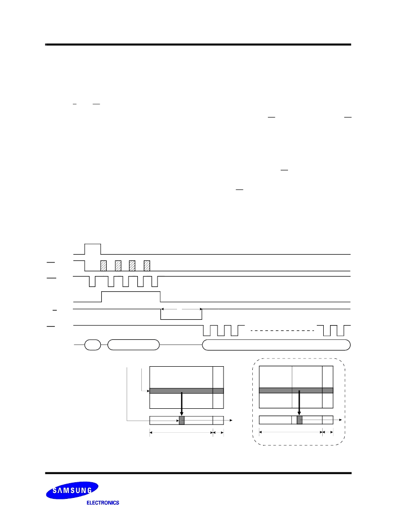
Figure 8-1. Read1 Operation
Start Add.(4Cycle)
00h
Data Output(Sequential)
CE
CLE
ALE
R/B
WE
I/O
0
~
7
RE
t
R
A
0
~ A
7
& A
9
~ A
27
(00h Command)
Data Field
Spare Field
Main array
(01h Command)
Data Field
Spare Field
1st half array
2st half array
NOTE :
1) After data access on 2nd half array by 01h command, the start pointer is automatically moved to 1st half array (00h) at next cycle.
1)
相關(guān)PDF資料 |
PDF描述 |
|---|---|
| K9E2G08U0M-Y | 256M x 8 Bits NAND Flash Memory |
| K9E2G08U0M-F | 256M x 8 Bits NAND Flash Memory |
| K9E2G08U0M-P | 256M x 8 Bits NAND Flash Memory |
| K9F1208D0A | 64M x 8 Bit , 32M x 16 Bit NAND Flash Memory |
| K9F1208D0A-P | TV 128C 128#22D PIN RECP |
相關(guān)代理商/技術(shù)參數(shù) |
參數(shù)描述 |
|---|---|
| K9E2G08U0M-Y | 制造商:SAMSUNG 制造商全稱:Samsung semiconductor 功能描述:256M x 8 Bits NAND Flash Memory |
| K9F1208B0B | 制造商:SAMSUNG 制造商全稱:Samsung semiconductor 功能描述:FLASH MEMORY |
| K9F1208B0C | 制造商:SAMSUNG 制造商全稱:Samsung semiconductor 功能描述:64M x 8 Bits NAND Flash Memory |
| K9F1208B0C-P | 制造商:SAMSUNG 制造商全稱:Samsung semiconductor 功能描述:FLASH MEMORY |
| K9F1208D0A | 制造商:SAMSUNG 制造商全稱:Samsung semiconductor 功能描述:64M x 8 Bit , 32M x 16 Bit NAND Flash Memory |
發(fā)布緊急采購(gòu),3分鐘左右您將得到回復(fù)。