- 您現(xiàn)在的位置:買賣IC網(wǎng) > PDF目錄373086 > K9E2G08U0M-V (SAMSUNG SEMICONDUCTOR CO. LTD.) 256M x 8 Bits NAND Flash Memory PDF資料下載
參數(shù)資料
| 型號(hào): | K9E2G08U0M-V |
| 廠商: | SAMSUNG SEMICONDUCTOR CO. LTD. |
| 英文描述: | 256M x 8 Bits NAND Flash Memory |
| 中文描述: | 256M x 8位NAND閃存 |
| 文件頁數(shù): | 30/38頁 |
| 文件大小: | 888K |
| 代理商: | K9E2G08U0M-V |
第1頁第2頁第3頁第4頁第5頁第6頁第7頁第8頁第9頁第10頁第11頁第12頁第13頁第14頁第15頁第16頁第17頁第18頁第19頁第20頁第21頁第22頁第23頁第24頁第25頁第26頁第27頁第28頁第29頁當(dāng)前第30頁第31頁第32頁第33頁第34頁第35頁第36頁第37頁第38頁
FLASH MEMORY
30
K9E2G08U0M
Preliminary
Figure 12. Block Erase Operation
BLOCK ERASE
The Erase operation is done on a block(16K Bytes) basis. Block address loading is accomplished in three cycles initiated by an
Erase Setup command(60h). Only address A
14
to A
27
is valid while A
9
to A
13
is ignored. The Erase Confirm command(D0h) following
the block address loading initiates the internal erasing process. This two-step sequence of setup followed by execution command
ensures that memory contents are not accidentally erased due to external noise conditions.
At the rising edge of WE after the erase confirm command input, the internal write controller handles erase and erase-verify. When
the erase operation is completed, the Write Status Bit(I/O 0) may be checked. Figure 12 details the sequence.
60h
Block Add. : A
14
~ A
27
I/O
X
R/B
Address Input(3Cycle)
I/O
0
Pass
D0h
70h
Fail
t
BERS
Multi-Plane Page Program into Plane 0~3 or Plane 4~7
Multi-Plane Page Program is an extension of Page Program, which is executed for a single plane with 528 bytes page register. Since
the device is equipped with four memory planes, activating the four sets of 528 bytes page register enables a simultaneous program-
ming of four pages. Partial activation of four planes is also permitted.
After writing the first set of data up to 528 byte into the selected page register, Dummy Page Program command (11h) instead of
actual Page Program (10h) is inputted to finish data-loading of the current plane and move to the next plane. Since no programming
process is involved, R/B remains in Busy state for a short period of time(tDBSY). Read Status command (standard 70h or alternate
71h) may be issued to find out when the device returns to Ready state by polling the Ready/Busy status bit(I/O 6). Then the next set
of data for one of the other planes is inputted with the same command and address sequences. After inputting data for the last plane,
actual True Page Program (10h) instead of dumy Page Program command (11h) must be followed to start the programming process.
The operation of R/B and Read Status is the same as that of Page Program. Since maximum four pages are programmed simulta-
neously, pass/fail status is available for each page when the program operation completes. The extended status bits (I/O1 through I/
O 4) are checked by inputting the Read Multi-Plane Status Register. Status bit of I/O 0 is set to "1" when any of the pages fails. Multi-
Plane page Program with "01h" pointer is not supported, thus prohibited.
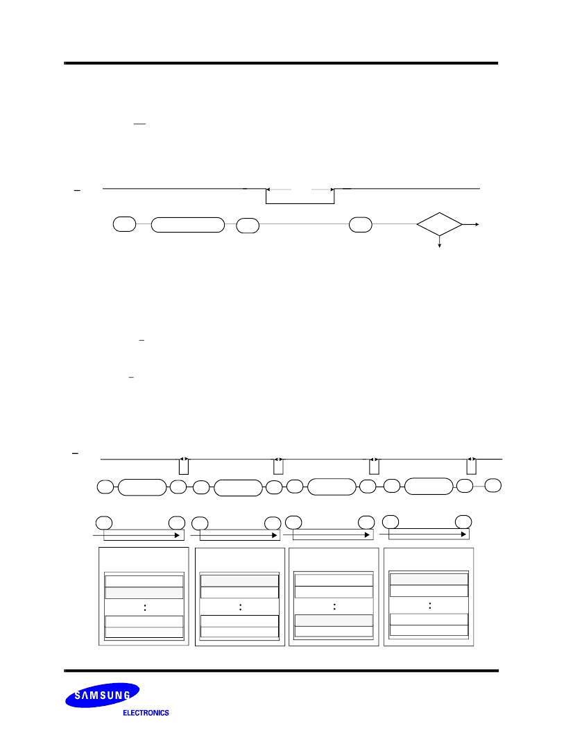
Figure 13. Four-Plane Page Program
80h
11h
80h
11h
80h
11h
80h
10h
Data
Input
Plane 0
(2,048 Blocks)
Plane 1
(2,048 Blocks)
Plane 2
(2,048 Blocks)
Plane 3
(2,048 Blocks)
Block 0
Block 4
Block 8,188
Block 8,184
Block 1
Block 5
Block 8,189
Block 8,185
Block 2
Block 6
Block 8,190
Block 8,186
Block 3
Block 7
Block 8,191
Block 8,187
80h
A
0
~ A
7
& A
9
~ A
27
528 bytes
I/O
X
R/B
Address &
Data Input
11h
80h
Address &
Data Input
11h
80h
Address &
Data Input
11h
80h
Address &
Data Input
10h
t
DBSY
t
DBSY
t
DBSY
t
PROG
71h
相關(guān)PDF資料 |
PDF描述 |
|---|---|
| K9E2G08U0M-Y | 256M x 8 Bits NAND Flash Memory |
| K9E2G08U0M-F | 256M x 8 Bits NAND Flash Memory |
| K9E2G08U0M-P | 256M x 8 Bits NAND Flash Memory |
| K9F1208D0A | 64M x 8 Bit , 32M x 16 Bit NAND Flash Memory |
| K9F1208D0A-P | TV 128C 128#22D PIN RECP |
相關(guān)代理商/技術(shù)參數(shù) |
參數(shù)描述 |
|---|---|
| K9E2G08U0M-Y | 制造商:SAMSUNG 制造商全稱:Samsung semiconductor 功能描述:256M x 8 Bits NAND Flash Memory |
| K9F1208B0B | 制造商:SAMSUNG 制造商全稱:Samsung semiconductor 功能描述:FLASH MEMORY |
| K9F1208B0C | 制造商:SAMSUNG 制造商全稱:Samsung semiconductor 功能描述:64M x 8 Bits NAND Flash Memory |
| K9F1208B0C-P | 制造商:SAMSUNG 制造商全稱:Samsung semiconductor 功能描述:FLASH MEMORY |
| K9F1208D0A | 制造商:SAMSUNG 制造商全稱:Samsung semiconductor 功能描述:64M x 8 Bit , 32M x 16 Bit NAND Flash Memory |
發(fā)布緊急采購,3分鐘左右您將得到回復(fù)。