- 您現(xiàn)在的位置:買賣IC網(wǎng) > PDF目錄373157 > KM44L32031BT-G(L)Y (SAMSUNG SEMICONDUCTOR CO. LTD.) DDR SDRAM Specification Version 1.0 PDF資料下載
參數(shù)資料
| 型號: | KM44L32031BT-G(L)Y |
| 廠商: | SAMSUNG SEMICONDUCTOR CO. LTD. |
| 英文描述: | DDR SDRAM Specification Version 1.0 |
| 中文描述: | DDR SDRAM的規(guī)范版本1.0 |
| 文件頁數(shù): | 23/53頁 |
| 文件大小: | 669K |
| 代理商: | KM44L32031BT-G(L)Y |
第1頁第2頁第3頁第4頁第5頁第6頁第7頁第8頁第9頁第10頁第11頁第12頁第13頁第14頁第15頁第16頁第17頁第18頁第19頁第20頁第21頁第22頁當前第23頁第24頁第25頁第26頁第27頁第28頁第29頁第30頁第31頁第32頁第33頁第34頁第35頁第36頁第37頁第38頁第39頁第40頁第41頁第42頁第43頁第44頁第45頁第46頁第47頁第48頁第49頁第50頁第51頁第52頁第53頁
- 23 -
REV. 1.0 November. 2. 2000
128Mb DDR SDRAM
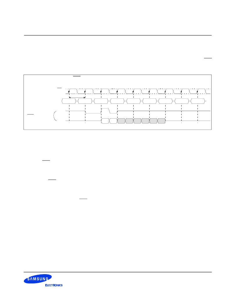
3.3.5 Read Interrupted by a Precharge
A Burst Read operation can be interrupted by precharge of the same bank. The minimum 1 clock is required
for the read to precharge intervals. A precharge command to output disable latency is equivalent to the CAS
latency.
Command
< Burst Length=8, CAS Latency=2 >
READ
NOP
Precharge
NOP
NOP
NOP
NOP
NOP
NOP
DQS
DQ
′
s
CAS Latency=2
Dout 0
Dout 1
Dout 2
Dout 3
Interrupted by precharge
2
0
1
5
3
4
8
6
7
Dout 4
Dout 5 Dout 6
Dout 7
1t
CK
CK
CK
When a burst Read command is issued to a DDR SDRAM, a Precharge command may be issued to the same
bank before the Read burst is complete. The following functionality determines when a Precharge command
may be given during a Read burst and when a new Bank Activate command may be issued to the same bank.
1. For the earliest possible Precharge command without interrupting a Read burst, the Precharge command
may be given on the rising clock edge which is CL clock cycles before the end of the Read burst where CL
is the CAS Latency. A new Bank Activate command may be issued to the same bank after tRP (RAS
Precharge time).
2. When a Precharge command interrupts a Read burst operation, the Precharge command may be given on
the rising clock edge which is CL clock cycles before the last data from the interrupted Read burst where
CL is the CAS Latency. Once the last data word has been output, the output buffers are tristated. A new
Bank Activate command may be issued to the same bank after tRP.
3. For a Read with autoprecharge command, a new Bank Activate command may be issued to the same
bank after tRP where tRP begins on the rising clock edge which is CL clock cycles before the end of the
Read burst where CL is the CAS Latency. During Read with autoprecharge, the initiation of the internal
precharge occurs at the same time as the earliest possible external Precharge command would initiate a
precharge operation without interrupting the Read burst as described in 1 above.
4. For all cases above, tRP is an analog delay that needs to be converted into clock cycles. The number of
clock cycles between a Precharge command and a new Bank Activate command to the same bank equals
tRP/tCK (where tCK is the clock cycle time) with the result rounded up to the nearest integer number of
clock cycles. (Note that rounding to X.5 is not possible since the Precharge and Bank Activate commands
can only be given on a
rising
clock edge).
In all cases, a Precharge operation cannot be initiated unless tRAS(min) [minimum Bank Activate to Precharge
time] has been satisfied. This includes Read with autoprecharge commands where tRAS(min) must still be
satisfied such that a Read with autoprecharge command has the same timing as a Read command followed by
the earliest possible Precharge command which does not interrupt the burst.
Figure 13. Read interrupted by a precharge timing
相關(guān)PDF資料 |
PDF描述 |
|---|---|
| KM48S2020C | 1M x 8Bit x 2 Banks Synchronous DRAM(1M x 8位 x 2組同步動態(tài)RAM) |
| KM48S8020B | 4M x 8Bit x 2 Banks Synchronous DRAM(4M x 8位 x 2組同步動態(tài)RAM) |
| KM48S8030D | 64Mbit SDRAM 2M x 8Bit x 4 Banks Synchronous DRAM LVTTL |
| KM48S8030 | 2M x 8Bit x 4 Banks Synchronous DRAM |
| KM48S8030C | 2M x 8Bit x 4 Banks Synchronous DRAM |
相關(guān)代理商/技術(shù)參數(shù) |
參數(shù)描述 |
|---|---|
| KM44L32031BT-GLZ/Y/0 | 制造商:SAMSUNG 制造商全稱:Samsung semiconductor 功能描述:DDR SDRAM Specification Version 1.0 |
| KM44S16020CT-G10 | 制造商:SEC 功能描述: |
| KM44S32030 | 制造商:SAMSUNG 制造商全稱:Samsung semiconductor 功能描述:8M x 4Bit x 4 Banks Synchronous DRAM |
| KM44S32030B | 制造商:SAMSUNG 制造商全稱:Samsung semiconductor 功能描述:128Mbit SDRAM 8M x 4Bit x 4 Banks Synchronous DRAM LVTTL |
| KM44S32030BT-G/F10 | 制造商:SAMSUNG 制造商全稱:Samsung semiconductor 功能描述:128Mbit SDRAM 8M x 4Bit x 4 Banks Synchronous DRAM LVTTL |
發(fā)布緊急采購,3分鐘左右您將得到回復(fù)。